

Key Insights
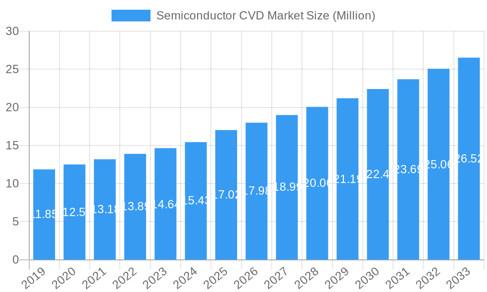
The global Semiconductor Chemical Vapor Deposition (CVD) market is poised for significant expansion, projected to reach 17.02 million units in 2025 and grow at a robust Compound Annual Growth Rate (CAGR) of 5.95% through 2033. This upward trajectory is primarily propelled by the escalating demand for advanced semiconductors across diverse industries, including automotive, consumer electronics, and telecommunications. The burgeoning development of Artificial Intelligence (AI), the Internet of Things (IoT), and 5G technologies necessitates increasingly sophisticated chip architectures, which in turn fuels the adoption of advanced CVD techniques for precise thin-film deposition. Key market drivers include the continuous miniaturization of transistors, the demand for higher performance and energy efficiency in electronic devices, and the ongoing research and development into novel materials and deposition processes. Furthermore, the increasing complexity of semiconductor manufacturing, requiring ultra-thin and uniform layers, makes CVD an indispensable technology.
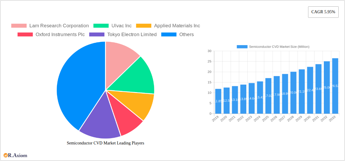
Semiconductor CVD Market Market Size (In Million)
The market segmentation reveals key application areas, with Foundry, Integrated Device Manufacturers (IDMs), and Memory Manufacturers being the primary consumers of CVD equipment. Foundries, in particular, are experiencing substantial growth due to the increasing fabless semiconductor model and the need for high-volume production of leading-edge chips. Trends such as the adoption of Atomic Layer Deposition (ALD) and Plasma-Enhanced CVD (PECVD) for depositing complex dielectric and metallic layers are shaping the market landscape. However, the market faces certain restraints, including the high capital expenditure required for advanced CVD systems and the increasing complexity of process integration. Despite these challenges, significant investment in research and development by leading companies like Lam Research Corporation, Applied Materials Inc., and Tokyo Electron Limited is expected to drive innovation and address these limitations, ensuring sustained market growth. The Asia Pacific region is anticipated to dominate the market, driven by the presence of major semiconductor manufacturing hubs.
Semiconductor CVD Market Company Market Share
This in-depth report provides a detailed analysis of the global Semiconductor Chemical Vapor Deposition (CVD) market, a critical technology underpinning the fabrication of advanced semiconductor devices. The market is witnessing significant growth driven by the insatiable demand for high-performance chips across various sectors, including consumer electronics, automotive, and artificial intelligence. Our study encompasses a comprehensive market analysis from the historical period of 2019–2024 through to a forecast period extending to 2033, with the base year and estimated year set at 2025. This report delves into market dynamics, key trends, technological advancements, competitive landscapes, and emerging opportunities within the Semiconductor CVD market, making it an indispensable resource for industry stakeholders, investors, and strategic planners. The estimated market size for Semiconductor CVD equipment is projected to reach $15,000 Million by 2025, with a Compound Annual Growth Rate (CAGR) of 8.5% expected throughout the forecast period.
Semiconductor CVD Market Market Concentration & Innovation
The Semiconductor CVD market is characterized by a moderate level of market concentration, with a few dominant players holding significant market share. Lam Research Corporation, Applied Materials Inc., and Tokyo Electron Limited are key players, collectively accounting for an estimated 65% of the global market share. Innovation remains a primary driver, fueled by the relentless pursuit of smaller, faster, and more energy-efficient semiconductor devices. Key innovation areas include the development of Atomic Layer Deposition (ALD) techniques integrated with CVD, enabling precise control over film thickness at the atomic scale, crucial for advanced node manufacturing. Regulatory frameworks, particularly those focused on environmental sustainability and safety standards for chemical usage in semiconductor fabrication, are also shaping product development and market entry strategies.
- Market Share Leaders (Estimated 2025):
- Lam Research Corporation: ~25%
- Applied Materials Inc.: ~23%
- Tokyo Electron Limited: ~17%
- Innovation Drivers:
- Advanced node scaling (e.g., sub-5nm fabrication).
- Development of novel precursor materials for improved film properties.
- Integration of AI and machine learning for process optimization.
- Increased demand for deposition techniques for 3D NAND and advanced logic devices.
- M&A Activities: While major consolidation has subsided, strategic partnerships and acquisitions focused on niche technologies or supply chain integration are anticipated, with estimated deal values in the range of $50 Million to $500 Million.
- Product Substitutes: While direct substitutes for CVD are limited given its fundamental role, advancements in PVD (Physical Vapor Deposition) and other thin-film deposition techniques can offer complementary or alternative solutions for specific applications.
- End-User Trends: Growing adoption of IoT devices, 5G infrastructure, electric vehicles, and AI accelerators are significantly boosting demand for advanced semiconductor manufacturing capabilities, thus driving CVD market growth.
Semiconductor CVD Market Industry Trends & Insights
The Semiconductor CVD market is experiencing robust growth, propelled by a confluence of technological advancements, escalating demand from burgeoning end-user industries, and strategic investments in semiconductor manufacturing capacity worldwide. The relentless miniaturization of transistors and the development of complex 3D architectures for memory and logic chips necessitate highly sophisticated CVD processes. Technologies like High-Volume Manufacturing (HVM) for advanced nodes, the increasing complexity of chip designs for AI and high-performance computing (HPC), and the critical role of CVD in the fabrication of advanced packaging solutions are key catalysts. The market penetration of next-generation semiconductor technologies, such as GaN (Gallium Nitride) and SiC (Silicon Carbide) for power electronics, is also creating new avenues for CVD equipment and process innovation, contributing to a projected market CAGR of 8.5%.
The industry is witnessing a significant trend towards miniaturization and enhanced performance, pushing the boundaries of deposition technology. CVD equipment manufacturers are investing heavily in research and development to offer solutions capable of depositing ultra-thin films with exceptional uniformity, conformality, and precise stoichiometry. This includes the development of single-wafer processing tools and multi-chamber systems that allow for sequential deposition of different materials, critical for creating advanced transistor gates, interconnects, and memory cells. The growing demand for advanced packaging techniques, such as 3D stacking and heterogeneous integration, also relies heavily on precise deposition processes, further bolstering the CVD market.
Consumer preferences for more powerful, energy-efficient, and feature-rich electronic devices are indirectly fueling the demand for advanced semiconductors, and consequently, for sophisticated CVD equipment. The automotive sector's rapid electrification and the increasing integration of advanced driver-assistance systems (ADAS) require high-performance power semiconductors and advanced processors, all manufactured using CVD processes. Similarly, the proliferation of 5G networks, cloud computing, and the burgeoning Internet of Things (IoT) ecosystem are creating an unprecedented demand for semiconductor chips across all performance tiers.
The competitive dynamics within the Semiconductor CVD market are intense, characterized by continuous innovation, strategic partnerships, and significant R&D expenditure by leading players. Companies are focused on developing equipment that can handle larger wafer sizes (e.g., 300mm and upcoming 450mm wafers), improve throughput, and reduce the cost of ownership for semiconductor manufacturers. Furthermore, the increasing complexity of semiconductor manufacturing has led to a greater emphasis on process control, metrology, and automation, areas where CVD equipment plays a crucial role. The market is also seeing a rise in demand for specialized CVD equipment tailored for emerging materials and applications, such as atomic layer deposition (ALD) for extreme ultraviolet (EUV) lithography mask blanks and advanced display technologies. The total market size for Semiconductor CVD equipment is estimated to reach $15,000 Million by 2025.
Dominant Markets & Segments in Semiconductor CVD Market
The global Semiconductor CVD market is segmented by application into Foundry, Integrated Device Manufacturer (IDM), and Memory Manufacturers. The Foundry segment currently holds the dominant position, driven by the massive outsourcing of semiconductor manufacturing by fabless design companies. The increasing complexity and capital intensity of advanced chip manufacturing have led to a proliferation of foundries dedicated to producing cutting-edge logic and memory chips. These foundries invest heavily in state-of-the-art CVD equipment to meet the stringent demands of their diverse customer base, encompassing leading-edge process nodes and advanced materials. The sheer volume of wafer starts in foundries, especially for high-demand sectors like AI, HPC, and consumer electronics, solidifies its leadership.
- Key Drivers for Foundry Dominance:
- Economies of Scale: Foundries benefit from high-volume production, allowing for cost optimization of CVD processes.
- Technological Specialization: Foundries often specialize in advanced nodes and specific chip types, requiring tailored CVD solutions.
- Outsourcing Trend: The rise of fabless semiconductor companies fuels the growth of foundries.
- Infrastructure Investment: Significant global investment in new foundry capacity, particularly in Asia, bolsters demand.
The Integrated Device Manufacturer (IDM) segment also represents a significant portion of the market. IDMs design, manufacture, and sell their own semiconductor devices, maintaining in-house fabrication capabilities. This segment is characterized by its focus on proprietary technologies and specialized product lines, such as high-performance processors, analog ICs, and discrete components. IDMs continuously invest in upgrading their CVD equipment to maintain a competitive edge and ensure the quality and reliability of their products. Their ability to control the entire manufacturing process allows for deep integration of CVD into their unique technology roadmaps.
- Key Drivers for IDM Segment:
- Proprietary Technology: In-house manufacturing allows for the development and protection of unique chip designs and processes.
- Quality Control: Direct oversight of CVD processes ensures stringent quality and performance standards.
- Specialized Applications: IDMs often cater to niche markets requiring highly specialized semiconductor solutions.
- Strategic Autonomy: Maintaining in-house fabrication provides greater control over supply chains and production schedules.
The Memory Manufacturers segment, while a substantial contributor, is experiencing dynamic shifts due to the cyclical nature of the memory market. However, the relentless demand for higher storage densities and faster memory speeds in smartphones, data centers, and gaming consoles continues to drive innovation and investment in advanced CVD techniques. The fabrication of 3D NAND flash memory and advanced DRAM architectures heavily relies on precise and uniform deposition of multiple layers, making CVD equipment indispensable. The ongoing development of next-generation memory technologies ensures continued demand for sophisticated CVD solutions within this segment.
- Key Drivers for Memory Manufacturers Segment:
- 3D NAND and DRAM Advancement: The increasing complexity of memory cell structures requires advanced CVD capabilities.
- Data Growth: Exponential growth in data generation and consumption fuels demand for memory chips.
- Performance Enhancements: Continuous pursuit of higher memory speeds and lower power consumption.
- New Memory Technologies: Emerging memory types, such as MRAM and ReRAM, also leverage CVD processes.
Geographically, Asia Pacific stands out as the dominant region, primarily due to the concentration of major semiconductor manufacturing hubs in countries like Taiwan, South Korea, China, and Japan. Substantial government initiatives, substantial foreign direct investment, and a robust ecosystem of foundries, IDMs, and memory manufacturers contribute to its leadership. The region's dominance is further amplified by its role as the primary manufacturing base for consumer electronics, automotive components, and telecommunications equipment that rely heavily on semiconductors. North America and Europe also represent significant markets, driven by advanced research and development, specialized manufacturing, and the growing demand for semiconductors in the automotive and aerospace industries.
Semiconductor CVD Market Product Developments
The Semiconductor CVD market is characterized by continuous product innovations aimed at enhancing deposition precision, efficiency, and compatibility with advanced materials. Manufacturers are developing advanced CVD systems capable of ultra-thin film deposition with atomic-level control, crucial for sub-5nm logic nodes and high-density memory structures. These advancements include integrated plasma-enhanced CVD (PECVD) and atomic layer deposition (ALD) capabilities within single tools, offering superior film uniformity and conformality. Furthermore, the development of new precursor chemistries is enabling the deposition of novel materials with tailored electrical, thermal, and optical properties, essential for emerging applications in power electronics, advanced displays, and sensors. These product developments provide competitive advantages by enabling higher device performance, reduced power consumption, and lower manufacturing costs for semiconductor fabricators.
Report Scope & Segmentation Analysis
This report meticulously analyzes the Semiconductor CVD market across its key application segments: Foundry, Integrated Device Manufacturer (IDM), and Memory Manufacturers. The Foundry segment is projected to witness substantial growth, driven by the increasing demand for outsourced manufacturing of advanced logic and memory chips for AI, HPC, and IoT applications. Its market size is estimated to reach $7,500 Million by 2025. The Integrated Device Manufacturer (IDM) segment, while mature, continues to be a significant revenue generator, driven by the need for specialized chips in automotive, industrial, and defense sectors. This segment is expected to reach $4,500 Million by 2025. The Memory Manufacturers segment, though subject to market cycles, will see sustained demand for advanced CVD equipment to support the production of high-density 3D NAND and next-generation DRAM. This segment is projected to reach $3,000 Million by 2025, with continued growth expected as data demands escalate.
Key Drivers of Semiconductor CVD Market Growth
The Semiconductor CVD market is experiencing robust expansion driven by several pivotal factors. The escalating global demand for semiconductors across diverse industries, including AI, 5G, IoT, and automotive, is the primary growth catalyst. The relentless pursuit of Moore's Law, pushing for smaller and more powerful integrated circuits, necessitates advanced CVD techniques for fabricating intricate nanoscale structures. Significant investments in new wafer fabrication plants (fabs) worldwide, particularly in Asia, are directly translating into increased demand for CVD equipment. Furthermore, the growing adoption of advanced packaging technologies, which integrate multiple chips into a single package, relies heavily on precise thin-film deposition, a core capability of CVD. The development of next-generation materials like GaN and SiC for power electronics further fuels the need for specialized CVD solutions.
Challenges in the Semiconductor CVD Market Sector
Despite its strong growth trajectory, the Semiconductor CVD market faces several challenges. The extremely high capital expenditure required for advanced CVD equipment presents a significant barrier to entry for new players and can strain the finances of even established manufacturers. The complexity of semiconductor fabrication processes, including the need for precise control over deposition parameters and material properties, demands continuous and substantial R&D investment. Supply chain disruptions, particularly for specialized precursor chemicals and critical components, can impact production timelines and increase costs. Moreover, stringent environmental regulations concerning the use and disposal of chemicals used in CVD processes require ongoing compliance and innovation in greener technologies. Intense competition among a few dominant players also leads to pricing pressures.
Emerging Opportunities in Semiconductor CVD Market
The Semiconductor CVD market is ripe with emerging opportunities driven by technological advancements and evolving industry needs. The increasing adoption of advanced packaging techniques, such as 2.5D and 3D stacking, presents a significant opportunity for CVD equipment that can handle complex geometries and diverse materials. The rise of specialized semiconductor materials like Gallium Nitride (GaN) and Silicon Carbide (SiC) for high-power and high-frequency applications is creating new markets for tailored CVD solutions. Furthermore, the growing demand for semiconductors in emerging fields such as quantum computing, advanced sensing, and flexible electronics opens up new avenues for CVD innovation. The integration of AI and machine learning into CVD process control and optimization offers opportunities for improved efficiency, yield, and reduced downtime.
Leading Players in the Semiconductor CVD Market Market
- Lam Research Corporation
- Ulvac Inc
- Applied Materials Inc.
- Oxford Instruments Plc
- Tokyo Electron Limited
- Aixtron SE
- CVD Equipment Corporation
- Veeco Instruments Inc.
- Asm International
Key Developments in Semiconductor CVD Market Industry
- September 2021: Lam Research announced the expansion of its manufacturing footprint in Oregon with a new 45,000 square foot facility in Sherwood. The new facility is Lam's fifth manufacturing site in the United States. It will further enhance its resilience and ability to meet increasing customer demand as chip suppliers seek to scale up production.
- February 2021: Oxford Instruments Plasma Technology announced that it would relocate to a state-of-the-art manufacturing facility in Bristol, United Kingdom. Customers, who include the world's leading semiconductor device manufacturers and materials research organizations, are driving the migration. The new facility will feature 1,000m2 of ISO 5 and 6 class application laboratories with a full array of wafer processing options and advanced characterization/metrology technology.
Strategic Outlook for Semiconductor CVD Market Market
The strategic outlook for the Semiconductor CVD market remains exceptionally positive, driven by the indispensable role of CVD technology in the fabrication of virtually all modern semiconductor devices. The continued demand for advanced logic and memory chips, fueled by innovations in AI, 5G, IoT, and autonomous systems, will sustain the need for cutting-edge CVD equipment. Significant global investments in semiconductor manufacturing capacity, particularly in emerging markets, are poised to drive substantial revenue growth. Furthermore, the development of novel semiconductor materials and the increasing adoption of advanced packaging techniques will create new market opportunities and necessitate further innovation in CVD processes. Companies that focus on developing highly efficient, precise, and cost-effective CVD solutions, while also investing in R&D for next-generation technologies, will be well-positioned for long-term success in this dynamic and critical industry. The market is expected to reach an estimated $15,000 Million by 2025, with sustained growth anticipated through 2033.
Semiconductor CVD Market Segmentation
-
1. Application
- 1.1. Foundry
- 1.2. Integrated Device Manufacturer (idm)
- 1.3. Memory Manufacturers
Semiconductor CVD Market Segmentation By Geography
- 1. North America
- 2. Europe
- 3. Asia Pacific
- 4. Rest of The World
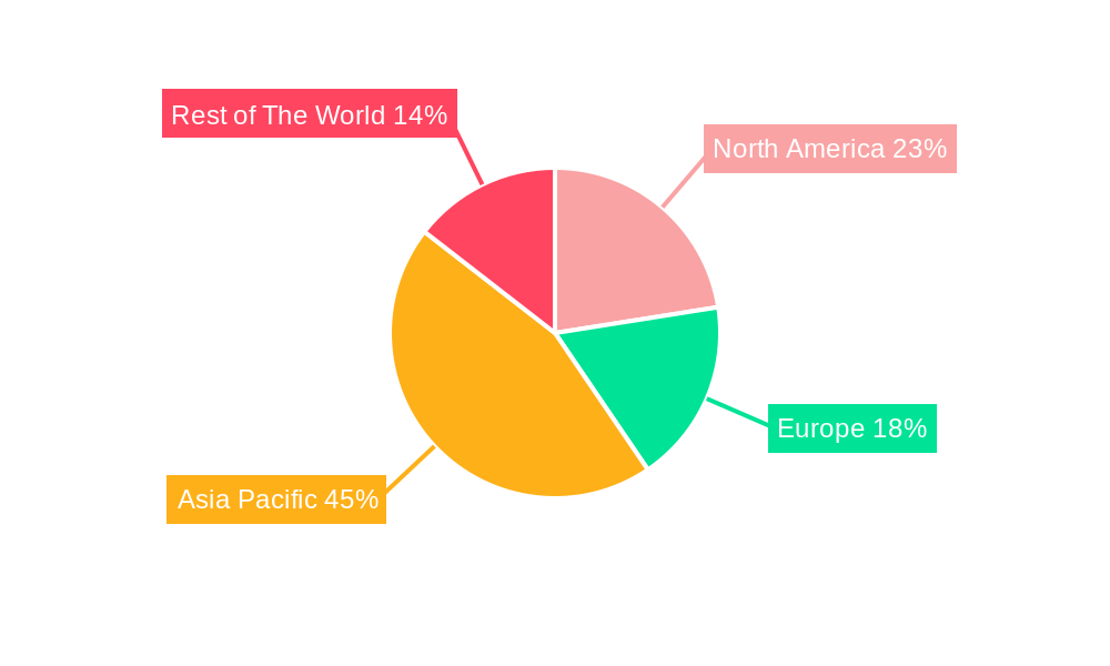
Semiconductor CVD Market Regional Market Share
Geographic Coverage of Semiconductor CVD Market
Semiconductor CVD Market REPORT HIGHLIGHTS
| Aspects | Details |
|---|---|
| Study Period | 2020-2034 |
| Base Year | 2025 |
| Estimated Year | 2026 |
| Forecast Period | 2026-2034 |
| Historical Period | 2020-2025 |
| Growth Rate | CAGR of 5.95% from 2020-2034 |
| Segmentation |
|
Table of Contents
- 1. Introduction
- 1.1. Research Scope
- 1.2. Market Segmentation
- 1.3. Research Objective
- 1.4. Definitions and Assumptions
- 2. Executive Summary
- 2.1. Market Snapshot
- 3. Market Dynamics
- 3.1. Market Drivers
- 3.2. Market Restrains
- 3.3. Market Trends
- 3.4. Market Opportunities
- 4. Market Factor Analysis
- 4.1. Porters Five Forces
- 4.1.1. Bargaining Power of Suppliers
- 4.1.2. Bargaining Power of Buyers
- 4.1.3. Threat of New Entrants
- 4.1.4. Threat of Substitutes
- 4.1.5. Competitive Rivalry
- 4.2. PESTEL analysis
- 4.3. BCG Analysis
- 4.3.1. Stars (High Growth, High Market Share)
- 4.3.2. Cash Cows (Low Growth, High Market Share)
- 4.3.3. Question Mark (High Growth, Low Market Share)
- 4.3.4. Dogs (Low Growth, Low Market Share)
- 4.4. Ansoff Matrix Analysis
- 4.5. Supply Chain Analysis
- 4.6. Regulatory Landscape
- 4.7. Current Market Potential and Opportunity Assessment (TAM–SAM–SOM Framework)
- 4.8. RAX Analyst Note
- 4.1. Porters Five Forces
- 5. Market Analysis, Insights and Forecast 2021-2033
- 5.1. Market Analysis, Insights and Forecast - by Application
- 5.1.1. Foundry
- 5.1.2. Integrated Device Manufacturer (idm)
- 5.1.3. Memory Manufacturers
- 5.2. Market Analysis, Insights and Forecast - by Region
- 5.2.1. North America
- 5.2.2. Europe
- 5.2.3. Asia Pacific
- 5.2.4. Rest of The World
- 5.1. Market Analysis, Insights and Forecast - by Application
- 6. Global Semiconductor CVD Market Analysis, Insights and Forecast, 2021-2033
- 6.1. Market Analysis, Insights and Forecast - by Application
- 6.1.1. Foundry
- 6.1.2. Integrated Device Manufacturer (idm)
- 6.1.3. Memory Manufacturers
- 6.1. Market Analysis, Insights and Forecast - by Application
- 7. North America Semiconductor CVD Market Analysis, Insights and Forecast, 2020-2032
- 7.1. Market Analysis, Insights and Forecast - by Application
- 7.1.1. Foundry
- 7.1.2. Integrated Device Manufacturer (idm)
- 7.1.3. Memory Manufacturers
- 7.1. Market Analysis, Insights and Forecast - by Application
- 8. Europe Semiconductor CVD Market Analysis, Insights and Forecast, 2020-2032
- 8.1. Market Analysis, Insights and Forecast - by Application
- 8.1.1. Foundry
- 8.1.2. Integrated Device Manufacturer (idm)
- 8.1.3. Memory Manufacturers
- 8.1. Market Analysis, Insights and Forecast - by Application
- 9. Asia Pacific Semiconductor CVD Market Analysis, Insights and Forecast, 2020-2032
- 9.1. Market Analysis, Insights and Forecast - by Application
- 9.1.1. Foundry
- 9.1.2. Integrated Device Manufacturer (idm)
- 9.1.3. Memory Manufacturers
- 9.1. Market Analysis, Insights and Forecast - by Application
- 10. Rest of The World Semiconductor CVD Market Analysis, Insights and Forecast, 2020-2032
- 10.1. Market Analysis, Insights and Forecast - by Application
- 10.1.1. Foundry
- 10.1.2. Integrated Device Manufacturer (idm)
- 10.1.3. Memory Manufacturers
- 10.1. Market Analysis, Insights and Forecast - by Application
- 11. Competitive Analysis
- 11.1. Company Profiles
- 11.1.1 Lam Research Corporation
- 11.1.1.1. Company Overview
- 11.1.1.2. Products
- 11.1.1.3. Company Financials
- 11.1.1.4. SWOT Analysis
- 11.1.2 Ulvac Inc
- 11.1.2.1. Company Overview
- 11.1.2.2. Products
- 11.1.2.3. Company Financials
- 11.1.2.4. SWOT Analysis
- 11.1.3 Applied Materials Inc
- 11.1.3.1. Company Overview
- 11.1.3.2. Products
- 11.1.3.3. Company Financials
- 11.1.3.4. SWOT Analysis
- 11.1.4 Oxford Instruments Plc
- 11.1.4.1. Company Overview
- 11.1.4.2. Products
- 11.1.4.3. Company Financials
- 11.1.4.4. SWOT Analysis
- 11.1.5 Tokyo Electron Limited
- 11.1.5.1. Company Overview
- 11.1.5.2. Products
- 11.1.5.3. Company Financials
- 11.1.5.4. SWOT Analysis
- 11.1.6 Aixtron Se
- 11.1.6.1. Company Overview
- 11.1.6.2. Products
- 11.1.6.3. Company Financials
- 11.1.6.4. SWOT Analysis
- 11.1.7 Cvd Equipment Corporation
- 11.1.7.1. Company Overview
- 11.1.7.2. Products
- 11.1.7.3. Company Financials
- 11.1.7.4. SWOT Analysis
- 11.1.8 Veeco Instruments Inc
- 11.1.8.1. Company Overview
- 11.1.8.2. Products
- 11.1.8.3. Company Financials
- 11.1.8.4. SWOT Analysis
- 11.1.9 Asm International
- 11.1.9.1. Company Overview
- 11.1.9.2. Products
- 11.1.9.3. Company Financials
- 11.1.9.4. SWOT Analysis
- 11.1.1 Lam Research Corporation
- 11.2. Market Entropy
- 11.2.1 Company's Key Areas Served
- 11.2.2 Recent Developments
- 11.3. Company Market Share Analysis 2025
- 11.3.1 Top 5 Companies Market Share Analysis
- 11.3.2 Top 3 Companies Market Share Analysis
- 11.4. List of Potential Customers
- 12. Research Methodology
List of Figures
- Figure 1: Global Semiconductor CVD Market Revenue Breakdown (Million, %) by Region 2025 & 2033
- Figure 2: Global Semiconductor CVD Market Volume Breakdown (K Unit, %) by Region 2025 & 2033
- Figure 3: North America Semiconductor CVD Market Revenue (Million), by Application 2025 & 2033
- Figure 4: North America Semiconductor CVD Market Volume (K Unit), by Application 2025 & 2033
- Figure 5: North America Semiconductor CVD Market Revenue Share (%), by Application 2025 & 2033
- Figure 6: North America Semiconductor CVD Market Volume Share (%), by Application 2025 & 2033
- Figure 7: North America Semiconductor CVD Market Revenue (Million), by Country 2025 & 2033
- Figure 8: North America Semiconductor CVD Market Volume (K Unit), by Country 2025 & 2033
- Figure 9: North America Semiconductor CVD Market Revenue Share (%), by Country 2025 & 2033
- Figure 10: North America Semiconductor CVD Market Volume Share (%), by Country 2025 & 2033
- Figure 11: Europe Semiconductor CVD Market Revenue (Million), by Application 2025 & 2033
- Figure 12: Europe Semiconductor CVD Market Volume (K Unit), by Application 2025 & 2033
- Figure 13: Europe Semiconductor CVD Market Revenue Share (%), by Application 2025 & 2033
- Figure 14: Europe Semiconductor CVD Market Volume Share (%), by Application 2025 & 2033
- Figure 15: Europe Semiconductor CVD Market Revenue (Million), by Country 2025 & 2033
- Figure 16: Europe Semiconductor CVD Market Volume (K Unit), by Country 2025 & 2033
- Figure 17: Europe Semiconductor CVD Market Revenue Share (%), by Country 2025 & 2033
- Figure 18: Europe Semiconductor CVD Market Volume Share (%), by Country 2025 & 2033
- Figure 19: Asia Pacific Semiconductor CVD Market Revenue (Million), by Application 2025 & 2033
- Figure 20: Asia Pacific Semiconductor CVD Market Volume (K Unit), by Application 2025 & 2033
- Figure 21: Asia Pacific Semiconductor CVD Market Revenue Share (%), by Application 2025 & 2033
- Figure 22: Asia Pacific Semiconductor CVD Market Volume Share (%), by Application 2025 & 2033
- Figure 23: Asia Pacific Semiconductor CVD Market Revenue (Million), by Country 2025 & 2033
- Figure 24: Asia Pacific Semiconductor CVD Market Volume (K Unit), by Country 2025 & 2033
- Figure 25: Asia Pacific Semiconductor CVD Market Revenue Share (%), by Country 2025 & 2033
- Figure 26: Asia Pacific Semiconductor CVD Market Volume Share (%), by Country 2025 & 2033
- Figure 27: Rest of The World Semiconductor CVD Market Revenue (Million), by Application 2025 & 2033
- Figure 28: Rest of The World Semiconductor CVD Market Volume (K Unit), by Application 2025 & 2033
- Figure 29: Rest of The World Semiconductor CVD Market Revenue Share (%), by Application 2025 & 2033
- Figure 30: Rest of The World Semiconductor CVD Market Volume Share (%), by Application 2025 & 2033
- Figure 31: Rest of The World Semiconductor CVD Market Revenue (Million), by Country 2025 & 2033
- Figure 32: Rest of The World Semiconductor CVD Market Volume (K Unit), by Country 2025 & 2033
- Figure 33: Rest of The World Semiconductor CVD Market Revenue Share (%), by Country 2025 & 2033
- Figure 34: Rest of The World Semiconductor CVD Market Volume Share (%), by Country 2025 & 2033
List of Tables
- Table 1: Global Semiconductor CVD Market Revenue Million Forecast, by Application 2020 & 2033
- Table 2: Global Semiconductor CVD Market Volume K Unit Forecast, by Application 2020 & 2033
- Table 3: Global Semiconductor CVD Market Revenue Million Forecast, by Region 2020 & 2033
- Table 4: Global Semiconductor CVD Market Volume K Unit Forecast, by Region 2020 & 2033
- Table 5: Global Semiconductor CVD Market Revenue Million Forecast, by Application 2020 & 2033
- Table 6: Global Semiconductor CVD Market Volume K Unit Forecast, by Application 2020 & 2033
- Table 7: Global Semiconductor CVD Market Revenue Million Forecast, by Country 2020 & 2033
- Table 8: Global Semiconductor CVD Market Volume K Unit Forecast, by Country 2020 & 2033
- Table 9: Global Semiconductor CVD Market Revenue Million Forecast, by Application 2020 & 2033
- Table 10: Global Semiconductor CVD Market Volume K Unit Forecast, by Application 2020 & 2033
- Table 11: Global Semiconductor CVD Market Revenue Million Forecast, by Country 2020 & 2033
- Table 12: Global Semiconductor CVD Market Volume K Unit Forecast, by Country 2020 & 2033
- Table 13: Global Semiconductor CVD Market Revenue Million Forecast, by Application 2020 & 2033
- Table 14: Global Semiconductor CVD Market Volume K Unit Forecast, by Application 2020 & 2033
- Table 15: Global Semiconductor CVD Market Revenue Million Forecast, by Country 2020 & 2033
- Table 16: Global Semiconductor CVD Market Volume K Unit Forecast, by Country 2020 & 2033
- Table 17: Global Semiconductor CVD Market Revenue Million Forecast, by Application 2020 & 2033
- Table 18: Global Semiconductor CVD Market Volume K Unit Forecast, by Application 2020 & 2033
- Table 19: Global Semiconductor CVD Market Revenue Million Forecast, by Country 2020 & 2033
- Table 20: Global Semiconductor CVD Market Volume K Unit Forecast, by Country 2020 & 2033
Frequently Asked Questions
1. What is the projected Compound Annual Growth Rate (CAGR) of the Semiconductor CVD Market?
The projected CAGR is approximately 5.95%.
2. Which companies are prominent players in the Semiconductor CVD Market?
Key companies in the market include Lam Research Corporation, Ulvac Inc, Applied Materials Inc, Oxford Instruments Plc, Tokyo Electron Limited, Aixtron Se, Cvd Equipment Corporation, Veeco Instruments Inc, Asm International.
3. What are the main segments of the Semiconductor CVD Market?
The market segments include Application.
4. Can you provide details about the market size?
The market size is estimated to be USD 17.02 Million as of 2022.
5. What are some drivers contributing to market growth?
Increase In Demand For Microelectronics And Semiconductor Devices; Rise In Application Of The Technology For Several End-users.
6. What are the notable trends driving market growth?
Increase in Demand for Microelectronics and Consumer Electronics to Fuel the Demand.
7. Are there any restraints impacting market growth?
Adaptability Requirements and Power Outages.
8. Can you provide examples of recent developments in the market?
September 2021 - Lam Research announced the expansion of its manufacturing footprint in Oregon with a new 45,000 square foot facility in Sherwood. The new facility is Lam's fifth manufacturing site in the United States. It will further enhance its resilience and ability to meet increasing customer demand as chip suppliers seek to scale up production.
9. What pricing options are available for accessing the report?
Pricing options include single-user, multi-user, and enterprise licenses priced at USD 4750, USD 5250, and USD 8750 respectively.
10. Is the market size provided in terms of value or volume?
The market size is provided in terms of value, measured in Million and volume, measured in K Unit.
11. Are there any specific market keywords associated with the report?
Yes, the market keyword associated with the report is "Semiconductor CVD Market," which aids in identifying and referencing the specific market segment covered.
12. How do I determine which pricing option suits my needs best?
The pricing options vary based on user requirements and access needs. Individual users may opt for single-user licenses, while businesses requiring broader access may choose multi-user or enterprise licenses for cost-effective access to the report.
13. Are there any additional resources or data provided in the Semiconductor CVD Market report?
While the report offers comprehensive insights, it's advisable to review the specific contents or supplementary materials provided to ascertain if additional resources or data are available.
14. How can I stay updated on further developments or reports in the Semiconductor CVD Market?
To stay informed about further developments, trends, and reports in the Semiconductor CVD Market, consider subscribing to industry newsletters, following relevant companies and organizations, or regularly checking reputable industry news sources and publications.
Methodology
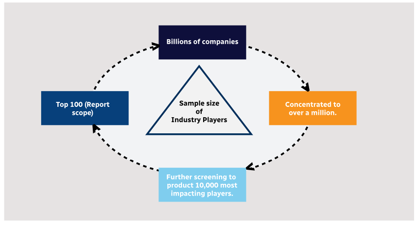
Step 1 - Identification of Relevant Samples Size from Population Database

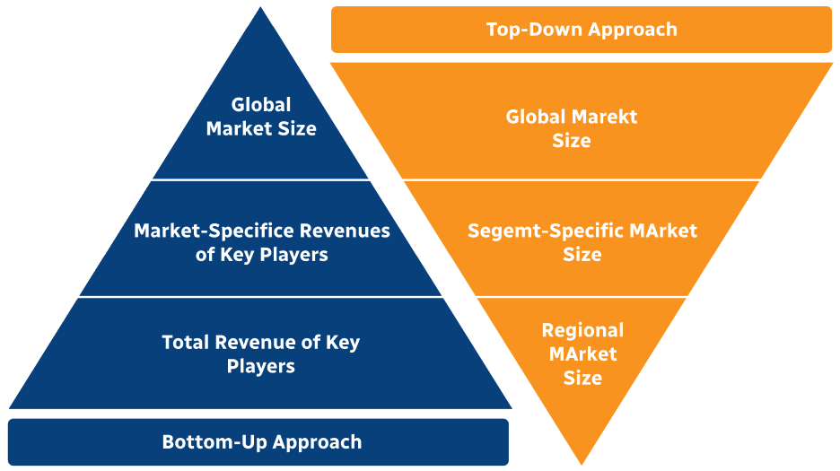
Step 2 - Approaches for Defining Global Market Size (Value, Volume* & Price*)
Note*: In applicable scenarios
Step 3 - Data Sources
Primary Research
- Web Analytics
- Survey Reports
- Research Institute
- Latest Research Reports
- Opinion Leaders
Secondary Research
- Annual Reports
- White Paper
- Latest Press Release
- Industry Association
- Paid Database
- Investor Presentations

Step 4 - Data Triangulation
Involves using different sources of information in order to increase the validity of a study
These sources are likely to be stakeholders in a program - participants, other researchers, program staff, other community members, and so on.
Then we put all data in single framework & apply various statistical tools to find out the dynamic on the market.
During the analysis stage, feedback from the stakeholder groups would be compared to determine areas of agreement as well as areas of divergence