

Key Insights
The global Semiconductor Lithography Equipment market is poised for robust expansion, projected to reach $26.48 million by 2025 and continue its upward trajectory with a Compound Annual Growth Rate (CAGR) of 7.38% through 2033. This significant growth is propelled by escalating demand for advanced semiconductor devices across various sectors, including consumer electronics, automotive, and telecommunications. The increasing complexity and miniaturization of integrated circuits necessitate sophisticated lithography techniques, driving innovation and investment in cutting-edge equipment. Key market drivers include the relentless pursuit of higher performance and greater energy efficiency in chips, the expanding Internet of Things (IoT) ecosystem, and the ongoing advancements in artificial intelligence (AI) and machine learning (ML) technologies, which rely heavily on powerful semiconductor processing. Furthermore, the growing adoption of 5G infrastructure worldwide is creating a substantial demand for high-performance chips, further fueling the lithography equipment market.
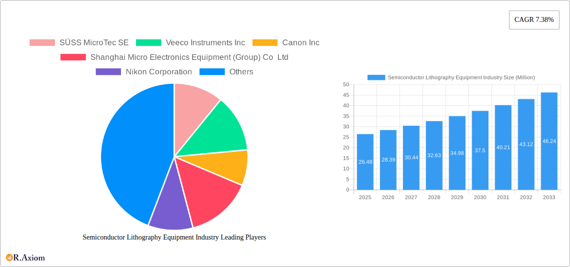
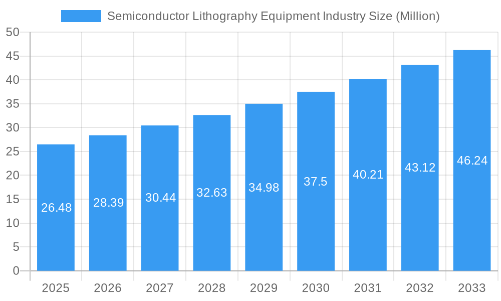
Semiconductor Lithography Equipment Industry Market Size (In Million)
The market's segmentation by type highlights the dominance and continued evolution of Extreme Ultraviolet Lithography (EUV) alongside Deep Ultraviolet Lithography (DUV), with EUV playing a crucial role in enabling the production of the most advanced nodes. In terms of applications, Advanced Packaging, MEMS Devices, and LED Devices represent key growth areas, each with unique lithographic requirements. While the market benefits from strong growth drivers, certain restraints, such as the high capital expenditure associated with advanced lithography systems and the complex manufacturing processes involved, may pose challenges. However, the industry's ability to innovate and adapt, coupled with strategic investments from major players like ASML Holding NV, will likely mitigate these restraints. The regional landscape is expected to be dominated by Asia, driven by its significant semiconductor manufacturing base, followed by North America and Europe, as global semiconductor supply chains continue to evolve.
Semiconductor Lithography Equipment Industry Company Market Share
Semiconductor Lithography Equipment Industry Market Concentration & Innovation
The semiconductor lithography equipment market exhibits a notable level of concentration, with a few dominant players controlling significant market share. This consolidation is driven by the immense capital investment required for research and development, particularly for advanced technologies like Extreme Ultraviolet Lithography (EUV). Innovation is a critical differentiator, with companies continually pushing the boundaries of resolution, throughput, and cost-effectiveness to meet the insatiable demand for smaller, more powerful chips. Regulatory frameworks, while evolving to support domestic chip manufacturing, also play a role in shaping market dynamics. Product substitutes are largely non-existent at the leading edge of semiconductor manufacturing, making lithography equipment indispensable. End-user trends, such as the proliferation of AI, 5G, and the Internet of Things (IoT), fuel the demand for increasingly sophisticated semiconductor devices, thereby driving innovation in lithography. Mergers and acquisitions (M&A) activities, though less frequent due to high valuations, are strategically undertaken to acquire critical technologies or expand market reach. For instance, the market share for advanced lithography solutions is heavily dominated by a few key vendors, with ASML Holding NV holding a substantial portion of the EUV market, estimated at over 85%. While specific M&A deal values fluctuate, strategic acquisitions in related areas, such as advanced packaging lithography, have seen investments in the hundreds of millions of dollars.
Semiconductor Lithography Equipment Industry Industry Trends & Insights
The semiconductor lithography equipment industry is experiencing robust growth, projected to achieve a Compound Annual Growth Rate (CAGR) of approximately 8.5% during the forecast period of 2025–2033. This expansion is propelled by several interconnected trends. The relentless demand for miniaturization and enhanced performance in electronic devices, driven by advancements in artificial intelligence (AI), autonomous driving, high-performance computing (HPC), and the expanding 5G infrastructure, necessitates the development and adoption of cutting-edge lithography solutions. The increasing complexity of semiconductor manufacturing processes, particularly the transition to advanced packaging techniques like chiplets, further fuels demand for specialized lithography equipment capable of high-resolution patterning and large-area exposure. Geopolitical shifts and government initiatives aimed at bolstering domestic semiconductor manufacturing capabilities are also significant growth catalysts, leading to increased investments in new fabrication facilities (fabs) and, consequently, lithography equipment. Technological disruptions, most notably the ongoing maturation and wider adoption of Extreme Ultraviolet Lithography (EUV), are reshaping the competitive landscape. EUV technology enables the creation of smaller transistor nodes, critical for next-generation processors. However, the high cost and complexity of EUV systems present a barrier to entry for some manufacturers. Deep Ultraviolet (DUV) lithography continues to be a workhorse for less advanced nodes and specific applications, with ongoing innovations in DUV systems improving their capabilities. Consumer preferences for faster, more energy-efficient, and feature-rich electronic devices indirectly drive the demand for advanced lithography that underpins these innovations. The competitive dynamics within the industry are characterized by intense R&D expenditure, strategic partnerships, and a continuous race to achieve technological superiority. Market penetration for advanced lithography, especially EUV, is steadily increasing as more foundries integrate these systems into their production lines. The market penetration for advanced lithography solutions is expected to reach approximately 60% by 2033, up from an estimated 30% in 2024, reflecting the growing adoption of next-generation chip designs.
Dominant Markets & Segments in Semiconductor Lithography Equipment Industry
Within the semiconductor lithography equipment industry, the market dominance is largely dictated by the technological sophistication and application breadth of different lithography types and their corresponding applications.
Deep Ultraviolet Lithography (DUV): DUV lithography remains a dominant segment due to its established maturity, cost-effectiveness, and widespread applicability across a vast range of semiconductor manufacturing processes. Its continued evolution, including advancements in illumination sources and optical systems, ensures its relevance for many critical applications. Key drivers for DUV's continued dominance include its lower capital expenditure compared to EUV, its proven reliability for producing billions of chips annually, and its essential role in manufacturing for consumer electronics, automotive, and industrial sectors where absolute bleeding-edge node technology is not always a prerequisite. The infrastructure for DUV is well-established globally, making it a cornerstone for many existing and new fabs.
Extreme Ultraviolet Lithography (EUV): EUV lithography represents the cutting edge of semiconductor lithography and is rapidly gaining dominance for the most advanced chip nodes. Its ability to achieve significantly smaller feature sizes (sub-10nm) is critical for high-performance processors used in AI, HPC, and next-generation mobile devices. The primary driver for EUV dominance is the demand for continuous miniaturization and performance enhancement in leading-edge semiconductors. Despite its high cost and technical challenges, the strategic importance of EUV for national semiconductor competitiveness is driving significant investment and adoption by major foundries like TSMC and Samsung. The market for EUV is projected for substantial growth, driven by the increasing complexity and performance demands of advanced integrated circuits.
Advanced Packaging: Advanced Packaging has emerged as a pivotal application segment, driving significant demand for specialized lithography solutions. This segment focuses on integrating multiple chips or components into a single package, improving performance, power efficiency, and form factor. The rise of chiplets, heterogeneous integration, and 3D stacking technologies are key drivers for advanced packaging. Lithography equipment optimized for larger exposure fields and higher resolution on substrates beyond traditional wafers are crucial here. Canon Inc.'s recent launch of an i-line lithography stepper specifically for 3D advanced packaging underscores the segment's importance and the development of tailored solutions to meet its unique requirements.
MEMS Devices: Micro-Electro-Mechanical Systems (MEMS) represent another significant application segment for lithography equipment. MEMS devices, used in a wide array of products from accelerometers in smartphones to sensors in automotive and medical applications, often require specialized lithography techniques to create their intricate mechanical structures. The growing adoption of MEMS in various industries, coupled with the need for precise and cost-effective manufacturing, sustains the demand for lithography equipment. EV Group's (EVG) continuous innovation in optical lithography solutions for MEMS and nanotechnology markets highlights the ongoing evolution and importance of this segment.
LED Devices: Lithography plays a crucial role in the manufacturing of Light Emitting Diodes (LEDs), particularly for achieving desired light output efficiency and color characteristics. While not as technologically demanding as cutting-edge logic chips, the sheer volume of LED production for lighting, displays, and automotive applications makes it a substantial market for lithography equipment. Innovations in LED lithography focus on improving throughput and reducing costs while maintaining precise patterning for enhanced device performance.
Semiconductor Lithography Equipment Industry Product Developments
Recent product developments in the semiconductor lithography equipment industry showcase a clear trend towards specialized solutions catering to evolving manufacturing needs. Canon Inc.'s launch of the FPA-5520iV LF2 i-line lithography stepper highlights advancements in back-end processing for 3D advanced packaging, enabling higher resolution (0.8-micron) over larger fields (52 mm by 68 mm, extendable to 100 mm by 100 mm) for chiplet integration. This demonstrates a strategic move towards supporting the complex demands of heterogeneous integration. Concurrently, EV Group (EVG) has strengthened its optical lithography portfolio with the next-generation 200-mm EVG 150 automated resist processing system. These developments underscore a focus on improved throughput, enhanced resolution, and greater flexibility to accommodate diverse application requirements, from advanced logic and memory to specialized areas like MEMS and advanced packaging. These innovations provide competitive advantages by enabling manufacturers to produce smaller, more powerful, and cost-effective semiconductor devices.
Report Scope & Segmentation Analysis
This report provides a comprehensive analysis of the global Semiconductor Lithography Equipment market, segmented by Type and Application. The study encompasses the historical period from 2019 to 2024, with a base year of 2025 and a forecast period extending to 2033. The segmentation by Type includes Deep Ultraviolet Lithography (DUV) and Extreme Ultraviolet Lithography (EUV), each with distinct market dynamics and growth trajectories driven by technological advancements and end-user demands. The segmentation by Application covers Advanced Packaging, MEMS Devices, and LED Devices, reflecting the diverse areas where lithography equipment is indispensable.
Deep Ultraviolet Lithography (DUV): This segment is expected to maintain a significant market share due to its established infrastructure and continued relevance for numerous semiconductor applications. Growth drivers include its cost-effectiveness and ongoing advancements in performance, making it crucial for high-volume manufacturing.
Extreme Ultraviolet Lithography (EUV): EUV is anticipated to experience the highest growth rate, fueled by the demand for leading-edge logic and memory chips. Investments by major foundries and government initiatives to advance semiconductor capabilities will drive market expansion.
Advanced Packaging: This application segment is projected for substantial growth as chiplet technology and heterogeneous integration become mainstream. Lithography solutions enabling larger exposure fields and higher precision for complex packaging designs will be in high demand.
MEMS Devices: The increasing adoption of MEMS sensors across various industries, from automotive to consumer electronics, will continue to drive demand for specialized lithography equipment that can precisely pattern micro-scale mechanical structures.
LED Devices: While a mature market, the ongoing demand for energy-efficient lighting and advanced display technologies will ensure continued steady growth for lithography equipment used in LED manufacturing, with a focus on cost-efficiency and improved performance.
Key Drivers of Semiconductor Lithography Equipment Industry Growth
The growth of the semiconductor lithography equipment industry is propelled by a confluence of powerful drivers. The relentless demand for miniaturization and increased performance in electronic devices, fueled by advancements in AI, IoT, and 5G, necessitates increasingly sophisticated lithography capabilities. Government initiatives worldwide aimed at bolstering domestic semiconductor manufacturing capacity, often termed "chip sovereignty," are leading to significant investments in new fabs and, consequently, lithography equipment. Technological advancements, particularly the maturation and wider adoption of Extreme Ultraviolet (EUV) lithography, are enabling the production of smaller and more powerful chips, driving demand for this cutting-edge technology. The growing complexity of semiconductor designs and the rise of advanced packaging techniques like chiplets further require specialized and highly precise lithography solutions.
Challenges in the Semiconductor Lithography Equipment Industry Sector
Despite its robust growth prospects, the semiconductor lithography equipment industry faces several significant challenges. The astronomical capital expenditure required for research, development, and manufacturing of advanced lithography systems, especially EUV, creates high barriers to entry and consolidation among a few key players. The complexity of these systems also leads to extended development cycles and stringent quality control requirements, posing supply chain risks. Regulatory hurdles and trade restrictions, particularly concerning the export of advanced semiconductor manufacturing technology, can impact global market access and collaboration. Furthermore, the intense competition among established players and the constant need for innovation to stay ahead of technological curves place immense pressure on R&D budgets and market share. The cost of ownership for advanced lithography tools remains a significant consideration for chip manufacturers, influencing adoption rates.
Emerging Opportunities in Semiconductor Lithography Equipment Industry
Emerging opportunities within the semiconductor lithography equipment industry are abundant, driven by evolving technological landscapes and market demands. The burgeoning field of neuromorphic computing and quantum computing, while still nascent, presents long-term opportunities for specialized lithography techniques to enable novel device architectures. The increasing demand for advanced packaging solutions, including wafer-level packaging and heterogeneous integration, is creating a growing market for lithography equipment tailored to these complex processes. Furthermore, the expansion of semiconductor manufacturing capabilities in emerging economies presents new market avenues for equipment suppliers. Innovations in photonics and optical sensing also require precise lithography for advanced component fabrication, opening up new application niches. The push for sustainable manufacturing practices within the semiconductor industry may also spur opportunities for equipment offering enhanced energy efficiency and reduced material waste.
Leading Players in the Semiconductor Lithography Equipment Industry Market
- ASML Holding NV
- Canon Inc.
- Nikon Corporation
- JEOL Ltd
- Shanghai Micro Electronics Equipment (Group) Co Ltd
- Veeco Instruments Inc
- SÜSS MicroTec SE
- Onto Innovation (Rudolph Technologies Inc)
- EV Group (EVG)
- Neutronix Quintel Inc (NXQ)
Key Developments in Semiconductor Lithography Equipment Industry Industry
- December 2022: Canon Inc. launched an i-line lithography stepper, the FPA-5520iV LF2, specifically for 3D advanced packaging applications, including chiplets on an interposer. This stepper, utilizing 365nm wavelength light, is optimized for back-end processing, delivering 0.8-micron resolution across a 52 mm by 68 mm single-exposure field, with a four-shot mode extending the area to 100 mm by 100 mm. This development addresses the growing need for high-resolution, large-area lithography in advanced packaging.
- November 2022: EV Group (EVG), a key player in lithography equipment and wafer bonding, enhanced its optical lithography solutions portfolio with the introduction of the next-generation 200-mm version of its EVG 150 automated resist processing system. This advancement strengthens EVG's offerings for the MEMS, nanotechnology, and semiconductor markets, focusing on improved processing capabilities for critical lithography steps.
Strategic Outlook for Semiconductor Lithography Equipment Industry Market
The strategic outlook for the semiconductor lithography equipment industry remains exceptionally strong, driven by the indispensable role of lithography in enabling continuous technological progress in semiconductors. The accelerating adoption of advanced technologies like AI, HPC, and 5G will continue to fuel the demand for more powerful and efficient chips, directly translating into increased demand for cutting-edge lithography solutions, particularly EUV. Geopolitical trends supporting domestic semiconductor manufacturing are likely to stimulate substantial investments in new fabrication facilities, creating significant market opportunities. Furthermore, the burgeoning field of advanced packaging presents a critical growth catalyst, requiring specialized lithography equipment for complex integration processes. Companies that can effectively innovate in terms of resolution, throughput, cost-effectiveness, and application-specific solutions will be well-positioned to capitalize on the industry's sustained growth and evolving demands.
Semiconductor Lithography Equipment Industry Segmentation
-
1. Type
- 1.1. Deep Ultraviolet Lithography (DUV)
- 1.2. Extreme Ultraviolet Lithography (EUV)
-
2. Application
- 2.1. Advanced Packaging
- 2.2. MEMS Devices
- 2.3. LED Devices
Semiconductor Lithography Equipment Industry Segmentation By Geography
- 1. North America
- 2. Europe
- 3. Asia
- 4. Australia and New Zealand
- 5. Latin America
- 6. Middle East and Africa
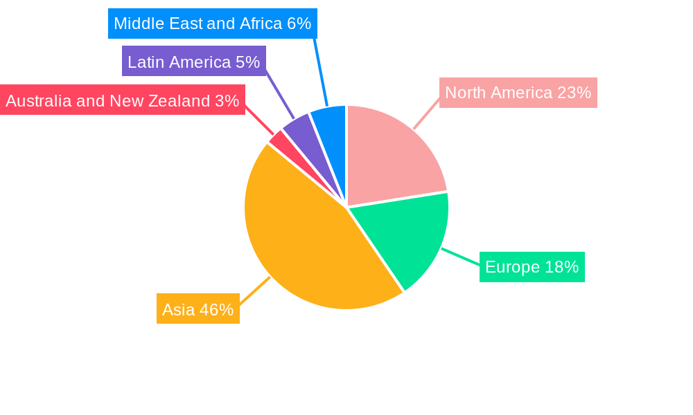
Semiconductor Lithography Equipment Industry Regional Market Share
Geographic Coverage of Semiconductor Lithography Equipment Industry
Semiconductor Lithography Equipment Industry REPORT HIGHLIGHTS
| Aspects | Details |
|---|---|
| Study Period | 2020-2034 |
| Base Year | 2025 |
| Estimated Year | 2026 |
| Forecast Period | 2026-2034 |
| Historical Period | 2020-2025 |
| Growth Rate | CAGR of 7.38% from 2020-2034 |
| Segmentation |
|
Table of Contents
- 1. Introduction
- 1.1. Research Scope
- 1.2. Market Segmentation
- 1.3. Research Objective
- 1.4. Definitions and Assumptions
- 2. Executive Summary
- 2.1. Market Snapshot
- 3. Market Dynamics
- 3.1. Market Drivers
- 3.2. Market Restrains
- 3.3. Market Trends
- 3.4. Market Opportunities
- 4. Market Factor Analysis
- 4.1. Porters Five Forces
- 4.1.1. Bargaining Power of Suppliers
- 4.1.2. Bargaining Power of Buyers
- 4.1.3. Threat of New Entrants
- 4.1.4. Threat of Substitutes
- 4.1.5. Competitive Rivalry
- 4.2. PESTEL analysis
- 4.3. BCG Analysis
- 4.3.1. Stars (High Growth, High Market Share)
- 4.3.2. Cash Cows (Low Growth, High Market Share)
- 4.3.3. Question Mark (High Growth, Low Market Share)
- 4.3.4. Dogs (Low Growth, Low Market Share)
- 4.4. Ansoff Matrix Analysis
- 4.5. Supply Chain Analysis
- 4.6. Regulatory Landscape
- 4.7. Current Market Potential and Opportunity Assessment (TAM–SAM–SOM Framework)
- 4.8. RAX Analyst Note
- 4.1. Porters Five Forces
- 5. Market Analysis, Insights and Forecast 2021-2033
- 5.1. Market Analysis, Insights and Forecast - by Type
- 5.1.1. Deep Ultraviolet Lithography (DUV)
- 5.1.2. Extreme Ultraviolet Lithography (EUV)
- 5.2. Market Analysis, Insights and Forecast - by Application
- 5.2.1. Advanced Packaging
- 5.2.2. MEMS Devices
- 5.2.3. LED Devices
- 5.3. Market Analysis, Insights and Forecast - by Region
- 5.3.1. North America
- 5.3.2. Europe
- 5.3.3. Asia
- 5.3.4. Australia and New Zealand
- 5.3.5. Latin America
- 5.3.6. Middle East and Africa
- 5.1. Market Analysis, Insights and Forecast - by Type
- 6. Global Semiconductor Lithography Equipment Industry Analysis, Insights and Forecast, 2021-2033
- 6.1. Market Analysis, Insights and Forecast - by Type
- 6.1.1. Deep Ultraviolet Lithography (DUV)
- 6.1.2. Extreme Ultraviolet Lithography (EUV)
- 6.2. Market Analysis, Insights and Forecast - by Application
- 6.2.1. Advanced Packaging
- 6.2.2. MEMS Devices
- 6.2.3. LED Devices
- 6.1. Market Analysis, Insights and Forecast - by Type
- 7. North America Semiconductor Lithography Equipment Industry Analysis, Insights and Forecast, 2020-2032
- 7.1. Market Analysis, Insights and Forecast - by Type
- 7.1.1. Deep Ultraviolet Lithography (DUV)
- 7.1.2. Extreme Ultraviolet Lithography (EUV)
- 7.2. Market Analysis, Insights and Forecast - by Application
- 7.2.1. Advanced Packaging
- 7.2.2. MEMS Devices
- 7.2.3. LED Devices
- 7.1. Market Analysis, Insights and Forecast - by Type
- 8. Europe Semiconductor Lithography Equipment Industry Analysis, Insights and Forecast, 2020-2032
- 8.1. Market Analysis, Insights and Forecast - by Type
- 8.1.1. Deep Ultraviolet Lithography (DUV)
- 8.1.2. Extreme Ultraviolet Lithography (EUV)
- 8.2. Market Analysis, Insights and Forecast - by Application
- 8.2.1. Advanced Packaging
- 8.2.2. MEMS Devices
- 8.2.3. LED Devices
- 8.1. Market Analysis, Insights and Forecast - by Type
- 9. Asia Semiconductor Lithography Equipment Industry Analysis, Insights and Forecast, 2020-2032
- 9.1. Market Analysis, Insights and Forecast - by Type
- 9.1.1. Deep Ultraviolet Lithography (DUV)
- 9.1.2. Extreme Ultraviolet Lithography (EUV)
- 9.2. Market Analysis, Insights and Forecast - by Application
- 9.2.1. Advanced Packaging
- 9.2.2. MEMS Devices
- 9.2.3. LED Devices
- 9.1. Market Analysis, Insights and Forecast - by Type
- 10. Australia and New Zealand Semiconductor Lithography Equipment Industry Analysis, Insights and Forecast, 2020-2032
- 10.1. Market Analysis, Insights and Forecast - by Type
- 10.1.1. Deep Ultraviolet Lithography (DUV)
- 10.1.2. Extreme Ultraviolet Lithography (EUV)
- 10.2. Market Analysis, Insights and Forecast - by Application
- 10.2.1. Advanced Packaging
- 10.2.2. MEMS Devices
- 10.2.3. LED Devices
- 10.1. Market Analysis, Insights and Forecast - by Type
- 11. Latin America Semiconductor Lithography Equipment Industry Analysis, Insights and Forecast, 2020-2032
- 11.1. Market Analysis, Insights and Forecast - by Type
- 11.1.1. Deep Ultraviolet Lithography (DUV)
- 11.1.2. Extreme Ultraviolet Lithography (EUV)
- 11.2. Market Analysis, Insights and Forecast - by Application
- 11.2.1. Advanced Packaging
- 11.2.2. MEMS Devices
- 11.2.3. LED Devices
- 11.1. Market Analysis, Insights and Forecast - by Type
- 12. Middle East and Africa Semiconductor Lithography Equipment Industry Analysis, Insights and Forecast, 2020-2032
- 12.1. Market Analysis, Insights and Forecast - by Type
- 12.1.1. Deep Ultraviolet Lithography (DUV)
- 12.1.2. Extreme Ultraviolet Lithography (EUV)
- 12.2. Market Analysis, Insights and Forecast - by Application
- 12.2.1. Advanced Packaging
- 12.2.2. MEMS Devices
- 12.2.3. LED Devices
- 12.1. Market Analysis, Insights and Forecast - by Type
- 13. Competitive Analysis
- 13.1. Company Profiles
- 13.1.1 SÜSS MicroTec SE
- 13.1.1.1. Company Overview
- 13.1.1.2. Products
- 13.1.1.3. Company Financials
- 13.1.1.4. SWOT Analysis
- 13.1.2 Veeco Instruments Inc
- 13.1.2.1. Company Overview
- 13.1.2.2. Products
- 13.1.2.3. Company Financials
- 13.1.2.4. SWOT Analysis
- 13.1.3 Canon Inc
- 13.1.3.1. Company Overview
- 13.1.3.2. Products
- 13.1.3.3. Company Financials
- 13.1.3.4. SWOT Analysis
- 13.1.4 Shanghai Micro Electronics Equipment (Group) Co Ltd
- 13.1.4.1. Company Overview
- 13.1.4.2. Products
- 13.1.4.3. Company Financials
- 13.1.4.4. SWOT Analysis
- 13.1.5 Nikon Corporation
- 13.1.5.1. Company Overview
- 13.1.5.2. Products
- 13.1.5.3. Company Financials
- 13.1.5.4. SWOT Analysis
- 13.1.6 JEOL Ltd
- 13.1.6.1. Company Overview
- 13.1.6.2. Products
- 13.1.6.3. Company Financials
- 13.1.6.4. SWOT Analysis
- 13.1.7 Neutronix Quintel Inc (NXQ)7 2 Vendor Market Share Analysi
- 13.1.7.1. Company Overview
- 13.1.7.2. Products
- 13.1.7.3. Company Financials
- 13.1.7.4. SWOT Analysis
- 13.1.8 Onto Innovation (Rudolph Technologies Inc )
- 13.1.8.1. Company Overview
- 13.1.8.2. Products
- 13.1.8.3. Company Financials
- 13.1.8.4. SWOT Analysis
- 13.1.9 ASML Holding NV
- 13.1.9.1. Company Overview
- 13.1.9.2. Products
- 13.1.9.3. Company Financials
- 13.1.9.4. SWOT Analysis
- 13.1.10 EV Group (EVG)
- 13.1.10.1. Company Overview
- 13.1.10.2. Products
- 13.1.10.3. Company Financials
- 13.1.10.4. SWOT Analysis
- 13.1.1 SÜSS MicroTec SE
- 13.2. Market Entropy
- 13.2.1 Company's Key Areas Served
- 13.2.2 Recent Developments
- 13.3. Company Market Share Analysis 2025
- 13.3.1 Top 5 Companies Market Share Analysis
- 13.3.2 Top 3 Companies Market Share Analysis
- 13.4. List of Potential Customers
- 14. Research Methodology
List of Figures
- Figure 1: Global Semiconductor Lithography Equipment Industry Revenue Breakdown (Million, %) by Region 2025 & 2033
- Figure 2: Global Semiconductor Lithography Equipment Industry Volume Breakdown (K Unit, %) by Region 2025 & 2033
- Figure 3: North America Semiconductor Lithography Equipment Industry Revenue (Million), by Type 2025 & 2033
- Figure 4: North America Semiconductor Lithography Equipment Industry Volume (K Unit), by Type 2025 & 2033
- Figure 5: North America Semiconductor Lithography Equipment Industry Revenue Share (%), by Type 2025 & 2033
- Figure 6: North America Semiconductor Lithography Equipment Industry Volume Share (%), by Type 2025 & 2033
- Figure 7: North America Semiconductor Lithography Equipment Industry Revenue (Million), by Application 2025 & 2033
- Figure 8: North America Semiconductor Lithography Equipment Industry Volume (K Unit), by Application 2025 & 2033
- Figure 9: North America Semiconductor Lithography Equipment Industry Revenue Share (%), by Application 2025 & 2033
- Figure 10: North America Semiconductor Lithography Equipment Industry Volume Share (%), by Application 2025 & 2033
- Figure 11: North America Semiconductor Lithography Equipment Industry Revenue (Million), by Country 2025 & 2033
- Figure 12: North America Semiconductor Lithography Equipment Industry Volume (K Unit), by Country 2025 & 2033
- Figure 13: North America Semiconductor Lithography Equipment Industry Revenue Share (%), by Country 2025 & 2033
- Figure 14: North America Semiconductor Lithography Equipment Industry Volume Share (%), by Country 2025 & 2033
- Figure 15: Europe Semiconductor Lithography Equipment Industry Revenue (Million), by Type 2025 & 2033
- Figure 16: Europe Semiconductor Lithography Equipment Industry Volume (K Unit), by Type 2025 & 2033
- Figure 17: Europe Semiconductor Lithography Equipment Industry Revenue Share (%), by Type 2025 & 2033
- Figure 18: Europe Semiconductor Lithography Equipment Industry Volume Share (%), by Type 2025 & 2033
- Figure 19: Europe Semiconductor Lithography Equipment Industry Revenue (Million), by Application 2025 & 2033
- Figure 20: Europe Semiconductor Lithography Equipment Industry Volume (K Unit), by Application 2025 & 2033
- Figure 21: Europe Semiconductor Lithography Equipment Industry Revenue Share (%), by Application 2025 & 2033
- Figure 22: Europe Semiconductor Lithography Equipment Industry Volume Share (%), by Application 2025 & 2033
- Figure 23: Europe Semiconductor Lithography Equipment Industry Revenue (Million), by Country 2025 & 2033
- Figure 24: Europe Semiconductor Lithography Equipment Industry Volume (K Unit), by Country 2025 & 2033
- Figure 25: Europe Semiconductor Lithography Equipment Industry Revenue Share (%), by Country 2025 & 2033
- Figure 26: Europe Semiconductor Lithography Equipment Industry Volume Share (%), by Country 2025 & 2033
- Figure 27: Asia Semiconductor Lithography Equipment Industry Revenue (Million), by Type 2025 & 2033
- Figure 28: Asia Semiconductor Lithography Equipment Industry Volume (K Unit), by Type 2025 & 2033
- Figure 29: Asia Semiconductor Lithography Equipment Industry Revenue Share (%), by Type 2025 & 2033
- Figure 30: Asia Semiconductor Lithography Equipment Industry Volume Share (%), by Type 2025 & 2033
- Figure 31: Asia Semiconductor Lithography Equipment Industry Revenue (Million), by Application 2025 & 2033
- Figure 32: Asia Semiconductor Lithography Equipment Industry Volume (K Unit), by Application 2025 & 2033
- Figure 33: Asia Semiconductor Lithography Equipment Industry Revenue Share (%), by Application 2025 & 2033
- Figure 34: Asia Semiconductor Lithography Equipment Industry Volume Share (%), by Application 2025 & 2033
- Figure 35: Asia Semiconductor Lithography Equipment Industry Revenue (Million), by Country 2025 & 2033
- Figure 36: Asia Semiconductor Lithography Equipment Industry Volume (K Unit), by Country 2025 & 2033
- Figure 37: Asia Semiconductor Lithography Equipment Industry Revenue Share (%), by Country 2025 & 2033
- Figure 38: Asia Semiconductor Lithography Equipment Industry Volume Share (%), by Country 2025 & 2033
- Figure 39: Australia and New Zealand Semiconductor Lithography Equipment Industry Revenue (Million), by Type 2025 & 2033
- Figure 40: Australia and New Zealand Semiconductor Lithography Equipment Industry Volume (K Unit), by Type 2025 & 2033
- Figure 41: Australia and New Zealand Semiconductor Lithography Equipment Industry Revenue Share (%), by Type 2025 & 2033
- Figure 42: Australia and New Zealand Semiconductor Lithography Equipment Industry Volume Share (%), by Type 2025 & 2033
- Figure 43: Australia and New Zealand Semiconductor Lithography Equipment Industry Revenue (Million), by Application 2025 & 2033
- Figure 44: Australia and New Zealand Semiconductor Lithography Equipment Industry Volume (K Unit), by Application 2025 & 2033
- Figure 45: Australia and New Zealand Semiconductor Lithography Equipment Industry Revenue Share (%), by Application 2025 & 2033
- Figure 46: Australia and New Zealand Semiconductor Lithography Equipment Industry Volume Share (%), by Application 2025 & 2033
- Figure 47: Australia and New Zealand Semiconductor Lithography Equipment Industry Revenue (Million), by Country 2025 & 2033
- Figure 48: Australia and New Zealand Semiconductor Lithography Equipment Industry Volume (K Unit), by Country 2025 & 2033
- Figure 49: Australia and New Zealand Semiconductor Lithography Equipment Industry Revenue Share (%), by Country 2025 & 2033
- Figure 50: Australia and New Zealand Semiconductor Lithography Equipment Industry Volume Share (%), by Country 2025 & 2033
- Figure 51: Latin America Semiconductor Lithography Equipment Industry Revenue (Million), by Type 2025 & 2033
- Figure 52: Latin America Semiconductor Lithography Equipment Industry Volume (K Unit), by Type 2025 & 2033
- Figure 53: Latin America Semiconductor Lithography Equipment Industry Revenue Share (%), by Type 2025 & 2033
- Figure 54: Latin America Semiconductor Lithography Equipment Industry Volume Share (%), by Type 2025 & 2033
- Figure 55: Latin America Semiconductor Lithography Equipment Industry Revenue (Million), by Application 2025 & 2033
- Figure 56: Latin America Semiconductor Lithography Equipment Industry Volume (K Unit), by Application 2025 & 2033
- Figure 57: Latin America Semiconductor Lithography Equipment Industry Revenue Share (%), by Application 2025 & 2033
- Figure 58: Latin America Semiconductor Lithography Equipment Industry Volume Share (%), by Application 2025 & 2033
- Figure 59: Latin America Semiconductor Lithography Equipment Industry Revenue (Million), by Country 2025 & 2033
- Figure 60: Latin America Semiconductor Lithography Equipment Industry Volume (K Unit), by Country 2025 & 2033
- Figure 61: Latin America Semiconductor Lithography Equipment Industry Revenue Share (%), by Country 2025 & 2033
- Figure 62: Latin America Semiconductor Lithography Equipment Industry Volume Share (%), by Country 2025 & 2033
- Figure 63: Middle East and Africa Semiconductor Lithography Equipment Industry Revenue (Million), by Type 2025 & 2033
- Figure 64: Middle East and Africa Semiconductor Lithography Equipment Industry Volume (K Unit), by Type 2025 & 2033
- Figure 65: Middle East and Africa Semiconductor Lithography Equipment Industry Revenue Share (%), by Type 2025 & 2033
- Figure 66: Middle East and Africa Semiconductor Lithography Equipment Industry Volume Share (%), by Type 2025 & 2033
- Figure 67: Middle East and Africa Semiconductor Lithography Equipment Industry Revenue (Million), by Application 2025 & 2033
- Figure 68: Middle East and Africa Semiconductor Lithography Equipment Industry Volume (K Unit), by Application 2025 & 2033
- Figure 69: Middle East and Africa Semiconductor Lithography Equipment Industry Revenue Share (%), by Application 2025 & 2033
- Figure 70: Middle East and Africa Semiconductor Lithography Equipment Industry Volume Share (%), by Application 2025 & 2033
- Figure 71: Middle East and Africa Semiconductor Lithography Equipment Industry Revenue (Million), by Country 2025 & 2033
- Figure 72: Middle East and Africa Semiconductor Lithography Equipment Industry Volume (K Unit), by Country 2025 & 2033
- Figure 73: Middle East and Africa Semiconductor Lithography Equipment Industry Revenue Share (%), by Country 2025 & 2033
- Figure 74: Middle East and Africa Semiconductor Lithography Equipment Industry Volume Share (%), by Country 2025 & 2033
List of Tables
- Table 1: Global Semiconductor Lithography Equipment Industry Revenue Million Forecast, by Type 2020 & 2033
- Table 2: Global Semiconductor Lithography Equipment Industry Volume K Unit Forecast, by Type 2020 & 2033
- Table 3: Global Semiconductor Lithography Equipment Industry Revenue Million Forecast, by Application 2020 & 2033
- Table 4: Global Semiconductor Lithography Equipment Industry Volume K Unit Forecast, by Application 2020 & 2033
- Table 5: Global Semiconductor Lithography Equipment Industry Revenue Million Forecast, by Region 2020 & 2033
- Table 6: Global Semiconductor Lithography Equipment Industry Volume K Unit Forecast, by Region 2020 & 2033
- Table 7: Global Semiconductor Lithography Equipment Industry Revenue Million Forecast, by Type 2020 & 2033
- Table 8: Global Semiconductor Lithography Equipment Industry Volume K Unit Forecast, by Type 2020 & 2033
- Table 9: Global Semiconductor Lithography Equipment Industry Revenue Million Forecast, by Application 2020 & 2033
- Table 10: Global Semiconductor Lithography Equipment Industry Volume K Unit Forecast, by Application 2020 & 2033
- Table 11: Global Semiconductor Lithography Equipment Industry Revenue Million Forecast, by Country 2020 & 2033
- Table 12: Global Semiconductor Lithography Equipment Industry Volume K Unit Forecast, by Country 2020 & 2033
- Table 13: Global Semiconductor Lithography Equipment Industry Revenue Million Forecast, by Type 2020 & 2033
- Table 14: Global Semiconductor Lithography Equipment Industry Volume K Unit Forecast, by Type 2020 & 2033
- Table 15: Global Semiconductor Lithography Equipment Industry Revenue Million Forecast, by Application 2020 & 2033
- Table 16: Global Semiconductor Lithography Equipment Industry Volume K Unit Forecast, by Application 2020 & 2033
- Table 17: Global Semiconductor Lithography Equipment Industry Revenue Million Forecast, by Country 2020 & 2033
- Table 18: Global Semiconductor Lithography Equipment Industry Volume K Unit Forecast, by Country 2020 & 2033
- Table 19: Global Semiconductor Lithography Equipment Industry Revenue Million Forecast, by Type 2020 & 2033
- Table 20: Global Semiconductor Lithography Equipment Industry Volume K Unit Forecast, by Type 2020 & 2033
- Table 21: Global Semiconductor Lithography Equipment Industry Revenue Million Forecast, by Application 2020 & 2033
- Table 22: Global Semiconductor Lithography Equipment Industry Volume K Unit Forecast, by Application 2020 & 2033
- Table 23: Global Semiconductor Lithography Equipment Industry Revenue Million Forecast, by Country 2020 & 2033
- Table 24: Global Semiconductor Lithography Equipment Industry Volume K Unit Forecast, by Country 2020 & 2033
- Table 25: Global Semiconductor Lithography Equipment Industry Revenue Million Forecast, by Type 2020 & 2033
- Table 26: Global Semiconductor Lithography Equipment Industry Volume K Unit Forecast, by Type 2020 & 2033
- Table 27: Global Semiconductor Lithography Equipment Industry Revenue Million Forecast, by Application 2020 & 2033
- Table 28: Global Semiconductor Lithography Equipment Industry Volume K Unit Forecast, by Application 2020 & 2033
- Table 29: Global Semiconductor Lithography Equipment Industry Revenue Million Forecast, by Country 2020 & 2033
- Table 30: Global Semiconductor Lithography Equipment Industry Volume K Unit Forecast, by Country 2020 & 2033
- Table 31: Global Semiconductor Lithography Equipment Industry Revenue Million Forecast, by Type 2020 & 2033
- Table 32: Global Semiconductor Lithography Equipment Industry Volume K Unit Forecast, by Type 2020 & 2033
- Table 33: Global Semiconductor Lithography Equipment Industry Revenue Million Forecast, by Application 2020 & 2033
- Table 34: Global Semiconductor Lithography Equipment Industry Volume K Unit Forecast, by Application 2020 & 2033
- Table 35: Global Semiconductor Lithography Equipment Industry Revenue Million Forecast, by Country 2020 & 2033
- Table 36: Global Semiconductor Lithography Equipment Industry Volume K Unit Forecast, by Country 2020 & 2033
- Table 37: Global Semiconductor Lithography Equipment Industry Revenue Million Forecast, by Type 2020 & 2033
- Table 38: Global Semiconductor Lithography Equipment Industry Volume K Unit Forecast, by Type 2020 & 2033
- Table 39: Global Semiconductor Lithography Equipment Industry Revenue Million Forecast, by Application 2020 & 2033
- Table 40: Global Semiconductor Lithography Equipment Industry Volume K Unit Forecast, by Application 2020 & 2033
- Table 41: Global Semiconductor Lithography Equipment Industry Revenue Million Forecast, by Country 2020 & 2033
- Table 42: Global Semiconductor Lithography Equipment Industry Volume K Unit Forecast, by Country 2020 & 2033
Frequently Asked Questions
1. What is the projected Compound Annual Growth Rate (CAGR) of the Semiconductor Lithography Equipment Industry?
The projected CAGR is approximately 7.38%.
2. Which companies are prominent players in the Semiconductor Lithography Equipment Industry?
Key companies in the market include SÜSS MicroTec SE, Veeco Instruments Inc, Canon Inc, Shanghai Micro Electronics Equipment (Group) Co Ltd, Nikon Corporation, JEOL Ltd, Neutronix Quintel Inc (NXQ)7 2 Vendor Market Share Analysi, Onto Innovation (Rudolph Technologies Inc ), ASML Holding NV, EV Group (EVG).
3. What are the main segments of the Semiconductor Lithography Equipment Industry?
The market segments include Type, Application.
4. Can you provide details about the market size?
The market size is estimated to be USD 26.48 Million as of 2022.
5. What are some drivers contributing to market growth?
Increasing Demand for Miniaturization and Extra Functionality by Electric Vehicles and Advanced Mobile Devices; Growing Innovation by Specialist Equipment Vendors offering Brand New Lithography Tools.
6. What are the notable trends driving market growth?
Deep Ultraviolet Lithography (DUV) to Hold Major Market Share.
7. Are there any restraints impacting market growth?
Challenges Regarding Complexity of Pattern in Manufacturing Process.
8. Can you provide examples of recent developments in the market?
December 2022 - Canon Inc. launched an i-line lithography stepper for 3D advanced packaging, such as those used with chiplets mounted on an interposer. The FPA-5520iV LF2, based on 365nm wavelength light, is optimized for back-end processing and delivers 0.8-micron resolution across a 52 mm by 68 mm single-exposure field. A four-shot mode extends the area to 100 mm by 100 mm.
9. What pricing options are available for accessing the report?
Pricing options include single-user, multi-user, and enterprise licenses priced at USD 4750, USD 5250, and USD 8750 respectively.
10. Is the market size provided in terms of value or volume?
The market size is provided in terms of value, measured in Million and volume, measured in K Unit.
11. Are there any specific market keywords associated with the report?
Yes, the market keyword associated with the report is "Semiconductor Lithography Equipment Industry," which aids in identifying and referencing the specific market segment covered.
12. How do I determine which pricing option suits my needs best?
The pricing options vary based on user requirements and access needs. Individual users may opt for single-user licenses, while businesses requiring broader access may choose multi-user or enterprise licenses for cost-effective access to the report.
13. Are there any additional resources or data provided in the Semiconductor Lithography Equipment Industry report?
While the report offers comprehensive insights, it's advisable to review the specific contents or supplementary materials provided to ascertain if additional resources or data are available.
14. How can I stay updated on further developments or reports in the Semiconductor Lithography Equipment Industry?
To stay informed about further developments, trends, and reports in the Semiconductor Lithography Equipment Industry, consider subscribing to industry newsletters, following relevant companies and organizations, or regularly checking reputable industry news sources and publications.
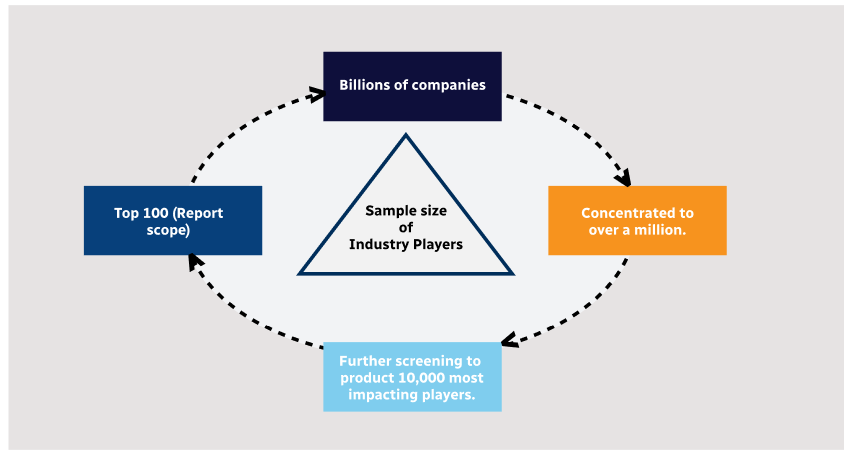
Methodology
Step 1 - Identification of Relevant Samples Size from Population Database

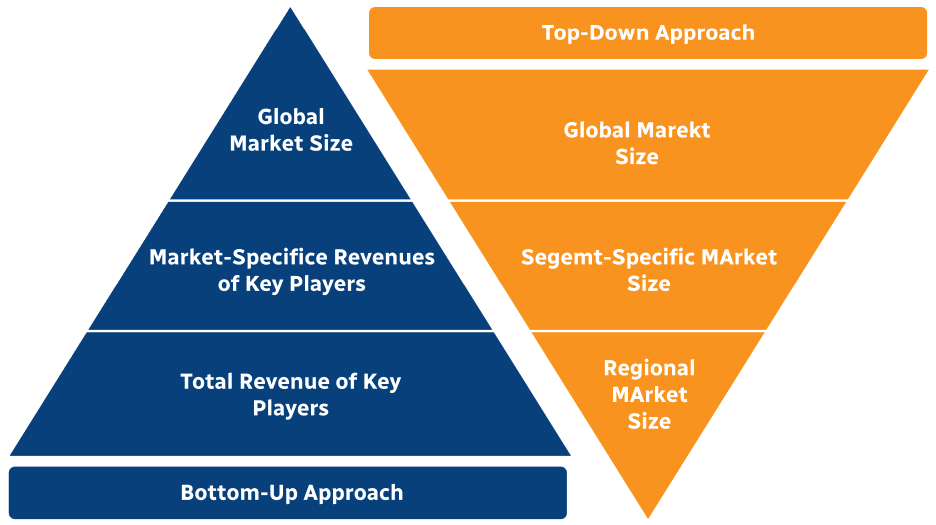
Step 2 - Approaches for Defining Global Market Size (Value, Volume* & Price*)
Note*: In applicable scenarios
Step 3 - Data Sources
Primary Research
- Web Analytics
- Survey Reports
- Research Institute
- Latest Research Reports
- Opinion Leaders
Secondary Research
- Annual Reports
- White Paper
- Latest Press Release
- Industry Association
- Paid Database
- Investor Presentations

Step 4 - Data Triangulation
Involves using different sources of information in order to increase the validity of a study
These sources are likely to be stakeholders in a program - participants, other researchers, program staff, other community members, and so on.
Then we put all data in single framework & apply various statistical tools to find out the dynamic on the market.
During the analysis stage, feedback from the stakeholder groups would be compared to determine areas of agreement as well as areas of divergence