

Key Insights
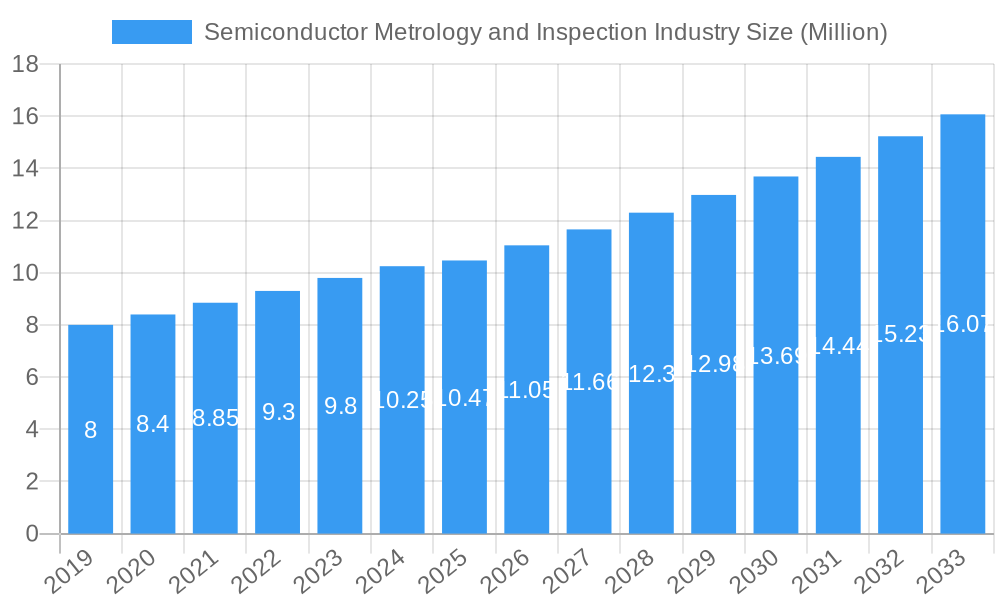
The Semiconductor Metrology and Inspection Industry is poised for robust expansion, projected to reach a substantial market size of USD 10.47 billion. This growth is fueled by a Compound Annual Growth Rate (CAGR) of 5.20%, indicating a steady and significant upward trajectory through the forecast period of 2025-2033. The industry's vitality is driven by the relentless pursuit of enhanced semiconductor performance, miniaturization, and the increasing complexity of integrated circuits. Key drivers include the burgeoning demand for advanced electronics across sectors like 5G, artificial intelligence, automotive, and the Internet of Things (IoT). As manufacturers strive for higher yields, reduced defect rates, and tighter process control, the need for sophisticated metrology and inspection solutions becomes paramount. Innovations in lithography, particularly the advancement towards EUV lithography, necessitate highly precise overlay measurement, critical dimension (CD) control, and defect analysis, thereby boosting the Lithography Metrology segment.
Semiconductor Metrology and Inspection Industry Market Size (In Million)
Furthermore, the escalating wafer fabrication complexity and the need to ensure wafer integrity throughout the manufacturing process underscore the importance of advanced Wafer Inspection systems. Thin Film Metrology is crucial for monitoring and controlling the deposition of ultra-thin layers essential for next-generation devices, while Other Process Control Systems integrate various data points to optimize manufacturing workflows. Geographically, the Asia Pacific region is expected to dominate the market, driven by the concentration of semiconductor manufacturing hubs and significant investments in advanced technology. North America and Europe will also contribute substantially, propelled by R&D initiatives and the presence of leading chip manufacturers. Restraints such as the high cost of advanced metrology equipment and the cyclical nature of the semiconductor industry might present challenges, but the overarching technological advancements and increasing demand for high-performance chips are expected to outweigh these limitations, ensuring sustained market growth.
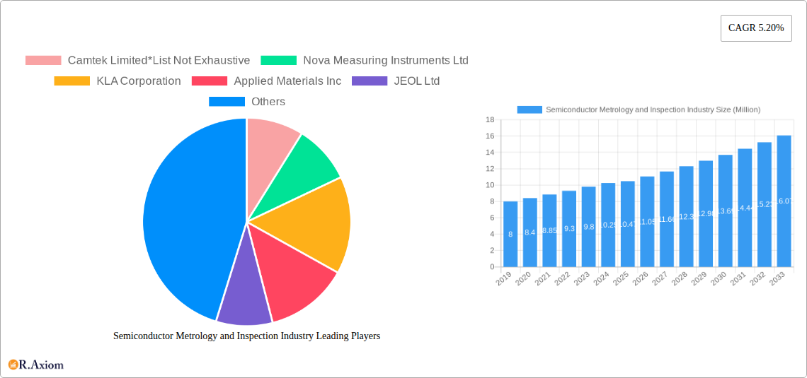
Semiconductor Metrology and Inspection Industry Company Market Share
This comprehensive report offers an in-depth analysis of the global Semiconductor Metrology and Inspection industry, covering the historical period from 2019 to 2024, the base year of 2025, and a detailed forecast period extending to 2033. With an estimated market size of over $15 Million in the base year, this sector is poised for significant expansion driven by advancements in semiconductor manufacturing and the ever-increasing demand for smaller, more powerful, and efficient electronic components. The report delves into market concentration, critical industry trends, dominant market segments, product innovations, growth drivers, challenges, emerging opportunities, and provides a detailed outlook for key players. High-traffic keywords such as "semiconductor metrology," "wafer inspection," "lithography metrology," "thin film metrology," "semiconductor inspection equipment," "process control systems," and "semiconductor manufacturing" are integrated throughout to maximize search engine visibility and reach industry professionals.
Semiconductor Metrology and Inspection Industry Market Concentration & Innovation
The Semiconductor Metrology and Inspection industry exhibits a moderate to high market concentration, dominated by a few key global players who command significant market share. KLA Corporation, Applied Materials Inc., and ASML Holding NV are prominent leaders, often holding combined market shares exceeding 60 Million. Innovation is the primary driver of market growth, fueled by the relentless pursuit of shrinking transistor sizes, enhanced performance, and reduced power consumption in semiconductors. Companies are heavily investing in Research and Development (R&D) to develop next-generation metrology and inspection solutions that can address the complex challenges of advanced nodes (e.g., 3nm, 2nm). Regulatory frameworks, particularly those related to semiconductor manufacturing standards and intellectual property, play a crucial role in shaping market dynamics. Product substitutes, while limited in the context of highly specialized metrology and inspection, can emerge in the form of alternative process control methods or integrated solutions. End-user trends are characterized by the increasing demand for higher yields, reduced defect rates, and faster time-to-market, necessitating sophisticated metrology and inspection capabilities. Mergers and Acquisitions (M&A) activities are strategic in nature, aimed at consolidating market position, acquiring cutting-edge technologies, and expanding product portfolios. M&A deal values can range from tens to hundreds of millions of dollars, reflecting the strategic importance of these transactions in the industry.
Semiconductor Metrology and Inspection Industry Industry Trends & Insights
The Semiconductor Metrology and Inspection industry is experiencing robust growth, projected to achieve a Compound Annual Growth Rate (CAGR) of approximately 7.5% over the forecast period. This expansion is underpinned by several key trends and insights. The relentless advancement of semiconductor technology, particularly the move towards advanced process nodes, is a significant market growth driver. As feature sizes shrink, the precision and sensitivity required for metrology and inspection escalate, demanding sophisticated solutions capable of detecting sub-nanometer defects and verifying critical dimension (CD) uniformity. Technological disruptions, such as the integration of Artificial Intelligence (AI) and Machine Learning (ML) into inspection algorithms, are revolutionizing defect detection and root cause analysis, leading to faster throughput and improved accuracy. Consumer preferences for smaller, more powerful, and energy-efficient electronic devices across various sectors—including smartphones, automotive, data centers, and IoT—directly translate into increased demand for high-performance semiconductors, thereby fueling the need for advanced metrology and inspection. Competitive dynamics are intense, with companies continuously innovating to maintain their technological edge and secure market share. The report anticipates a market penetration of advanced electron microscopy techniques and multi-modal inspection systems to rise significantly. Furthermore, the growing complexity of 3D chip architectures and advanced packaging technologies presents new challenges and opportunities for metrology and inspection providers. The increasing adoption of EUV lithography also necessitates highly specialized metrology and inspection solutions for mask blank and mask pattern inspection, as well as for overlay and focus control. The global semiconductor supply chain's strategic importance and the ongoing efforts to diversify manufacturing locations also contribute to market dynamics, creating demand for localized metrology and inspection capabilities. The shift towards heterogeneous integration and advanced packaging techniques further amplifies the need for specialized inspection tools to ensure the integrity and performance of these complex assemblies.
Dominant Markets & Segments in Semiconductor Metrology and Inspection Industry
The Lithography Metrology segment, encompassing Overlay, Dimension Equipment, and Mask Inspection and Metrology, currently dominates the Semiconductor Metrology and Inspection industry, representing a substantial portion of the market share, estimated to be over 35 Million in the base year. This dominance is driven by the critical role of lithography in defining semiconductor feature sizes and the increasing complexity of lithographic processes, especially with the advent of Extreme Ultraviolet (EUV) lithography.
- Lithography Metrology:
- Overlay Metrology: Essential for ensuring precise alignment between successive lithographic layers, crucial for device performance and yield. The demand for tighter overlay control in advanced nodes directly fuels this segment.
- Dimension Equipment (Critical Dimension Measurement): Verifying the exact dimensions of critical features on semiconductor wafers is paramount. Advancements in high-resolution metrology techniques are vital for maintaining precision at sub-nanometer scales.
- Mask Inspection and Metrology: Ensuring the defect-free nature of photomasks used in lithography is critical for preventing yield loss. The increasing complexity and cost of masks make this segment indispensable. Economic policies supporting domestic semiconductor manufacturing, such as tax incentives and subsidies, are major drivers for investment in lithography-related equipment.
Wafer Inspection is another significant segment, estimated to be valued at over 25 Million in the base year, focusing on detecting defects on the wafer surface at various stages of the manufacturing process.
- Wafer Inspection:
- Defect Detection: Identifying and classifying particles, pattern defects, and surface anomalies is crucial for maximizing wafer yield. Automation and AI-powered defect review are key trends.
- Yield Enhancement: By providing early detection of defects, wafer inspection systems contribute directly to improved manufacturing yields and reduced costs. Infrastructure development, including the expansion of semiconductor fabrication facilities (fabs), directly correlates with increased demand for wafer inspection solutions.
Thin Film Metrology plays a vital role in characterizing the properties of thin films deposited on wafers, essential for controlling device characteristics.
- Thin Film Metrology:
- Film Thickness and Composition Analysis: Precise measurement of film thickness, uniformity, and elemental composition is critical for a wide range of semiconductor devices. Advanced spectroscopic and ellipsometric techniques are key.
- Process Control: Accurate thin film characterization enables tighter control over deposition and etching processes, leading to improved device performance and reliability. Government initiatives focused on advanced materials research and development are indirectly bolstering this segment.
Other Process Control Systems encompass a broad range of solutions that monitor and control various aspects of the semiconductor manufacturing process beyond the core metrology and inspection functions.
- Other Process Control Systems:
- In-situ Monitoring: Real-time monitoring of process parameters within the fab environment enhances efficiency and predictability.
- Data Analytics for Process Optimization: Leveraging big data and analytics to identify process excursions and optimize manufacturing workflows. The growing emphasis on smart manufacturing and Industry 4.0 principles is a significant driver for this segment.
Geographically, Asia Pacific, particularly countries like Taiwan, South Korea, and China, is the dominant region due to its extensive semiconductor manufacturing base. North America and Europe also hold significant market share due to the presence of major chip designers and advanced R&D centers.
Semiconductor Metrology and Inspection Industry Product Developments
Recent product developments in the Semiconductor Metrology and Inspection industry are characterized by a focus on enhanced resolution, speed, and automation. Companies are introducing next-generation electron microscopes with higher magnification and improved contrast for nanoscale defect imaging. Advanced optical metrology systems are being developed to provide faster and more accurate measurements of critical dimensions and overlay. The integration of AI and machine learning algorithms is a key trend, enabling intelligent defect classification, root cause analysis, and predictive maintenance. These innovations offer significant competitive advantages by improving wafer yield, reducing manufacturing costs, and accelerating time-to-market for cutting-edge semiconductor devices.
Report Scope & Segmentation Analysis
This report meticulously analyzes the Semiconductor Metrology and Inspection industry across several key segments. The Lithography Metrology segment, including Overlay, Dimension Equipment, and Mask Inspection and Metrology, is projected to witness a CAGR of 8.0% over the forecast period, driven by the escalating demands of advanced lithography techniques. The Wafer Inspection segment is estimated to grow at a CAGR of 7.0%, fueled by the continuous need for defect reduction and yield enhancement in high-volume manufacturing. Thin Film Metrology is expected to expand at a CAGR of 6.5%, as precise characterization of thin films remains critical for device performance. The Other Process Control Systems segment, encompassing a range of solutions for overall fab efficiency, is anticipated to grow at a CAGR of 7.2%, reflecting the increasing adoption of smart manufacturing principles.
Key Drivers of Semiconductor Metrology and Inspection Industry Growth
The growth of the Semiconductor Metrology and Inspection industry is propelled by several interconnected factors. The escalating demand for advanced semiconductors, driven by 5G deployment, AI, autonomous vehicles, and IoT devices, necessitates continuous innovation in chip manufacturing, directly increasing the need for sophisticated metrology and inspection solutions. Technological advancements in semiconductor fabrication, particularly the transition to smaller process nodes (e.g., sub-10nm), demand higher precision and sensitivity in defect detection and measurement. Government initiatives and investments aimed at bolstering domestic semiconductor production and R&D, such as the CHIPS Act in the US and similar programs in Europe and Asia, are significantly boosting the market. The increasing complexity of integrated circuits and advanced packaging techniques also creates new challenges that require advanced metrology and inspection capabilities.
Challenges in the Semiconductor Metrology and Inspection Industry Sector
Despite robust growth, the Semiconductor Metrology and Inspection industry faces several challenges. The extremely high cost of advanced metrology and inspection equipment can be a barrier to entry for smaller manufacturers and research institutions. The rapid pace of technological advancement requires continuous and substantial R&D investment, posing a financial strain on companies. The global semiconductor supply chain, while strengthening, can still be subject to disruptions, impacting the availability of components for metrology and inspection equipment. Fierce competition among established players and emerging innovators can lead to price pressures and the need for constant differentiation. The stringent quality control requirements and the long development cycles for new semiconductor manufacturing processes also add complexity.
Emerging Opportunities in Semiconductor Metrology and Inspection Industry
Emerging opportunities in the Semiconductor Metrology and Inspection industry are abundant, driven by new technological frontiers and market demands. The rapid growth of the automotive semiconductor sector, requiring stringent reliability and safety standards, presents a significant opportunity for specialized metrology and inspection solutions. The burgeoning field of advanced packaging, including chiplets and 2.5D/3D integration, requires novel inspection techniques to ensure interconnect reliability and performance. The increasing adoption of AI and machine learning in chip design and manufacturing opens avenues for intelligent, data-driven metrology and inspection systems. The expansion of semiconductor manufacturing into new geographic regions, driven by supply chain diversification efforts, creates demand for localized metrology and inspection infrastructure and services.
Leading Players in the Semiconductor Metrology and Inspection Industry Market
- Camtek Limited
- Nova Measuring Instruments Ltd
- KLA Corporation
- Applied Materials Inc
- JEOL Ltd
- Hitachi Hi-Technologies Corporation (Hitachi Limited)
- Lasertec Corporation
- Nikon Metrology NV (Nikon Group)
- Thermo Fisher Scientific Inc
- Onto Innovation Inc
- ASML Holding NV
Key Developments in Semiconductor Metrology and Inspection Industry Industry
- 2023/2024: Introduction of AI-powered defect review and classification systems, significantly improving inspection throughput and accuracy.
- 2023: Launch of advanced e-beam metrology tools for sub-3nm node critical dimension measurements.
- 2022/2023: Increased focus on metrology solutions for advanced packaging technologies, including wafer-level packaging and heterogeneous integration.
- 2022: Strategic partnerships and M&A activities aimed at expanding product portfolios and market reach, with deal values often exceeding tens of millions of dollars.
- 2021/2022: Development of inline metrology solutions for real-time process monitoring and control, enhancing fab efficiency.
- 2020/2021: Significant R&D investments in next-generation lithography metrology to support the rollout of 5nm and 3nm semiconductor technologies.
Strategic Outlook for Semiconductor Metrology and Inspection Industry Market
The strategic outlook for the Semiconductor Metrology and Inspection industry is exceptionally strong, driven by the indispensable role of these technologies in enabling advanced semiconductor manufacturing. Continued innovation in metrology and inspection will be critical for the industry's growth, particularly in addressing the challenges of sub-nanometer nodes and complex 3D architectures. The increasing integration of AI and automation will further enhance the efficiency and effectiveness of inspection processes. Strategic collaborations and potential acquisitions are expected to continue as companies seek to broaden their technological capabilities and market access. The long-term trend of growing demand for sophisticated electronic devices across all sectors ensures a sustained need for cutting-edge metrology and inspection solutions, positioning the market for continued expansion and technological evolution.
Semiconductor Metrology and Inspection Industry Segmentation
-
1. Type
-
1.1. Lithography Metrology
- 1.1.1. Overlay
- 1.1.2. Dimension Equipment
- 1.1.3. Mask Inspection and Metrology
- 1.2. Wafer Inspection
- 1.3. Thin Film Metrology
- 1.4. Other Process Control Systems
-
1.1. Lithography Metrology
Semiconductor Metrology and Inspection Industry Segmentation By Geography
- 1. North America
- 2. Europe
- 3. Asia Pacific
- 4. Rest of the World
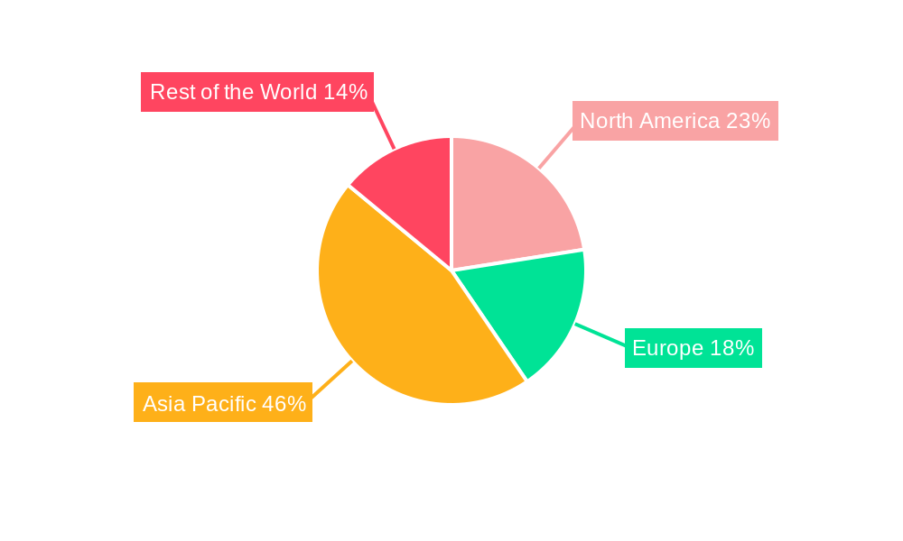
Semiconductor Metrology and Inspection Industry Regional Market Share
Geographic Coverage of Semiconductor Metrology and Inspection Industry
Semiconductor Metrology and Inspection Industry REPORT HIGHLIGHTS
| Aspects | Details |
|---|---|
| Study Period | 2020-2034 |
| Base Year | 2025 |
| Estimated Year | 2026 |
| Forecast Period | 2026-2034 |
| Historical Period | 2020-2025 |
| Growth Rate | CAGR of 5.20% from 2020-2034 |
| Segmentation |
|
Table of Contents
- 1. Introduction
- 1.1. Research Scope
- 1.2. Market Segmentation
- 1.3. Research Objective
- 1.4. Definitions and Assumptions
- 2. Executive Summary
- 2.1. Market Snapshot
- 3. Market Dynamics
- 3.1. Market Drivers
- 3.2. Market Restrains
- 3.3. Market Trends
- 3.4. Market Opportunities
- 4. Market Factor Analysis
- 4.1. Porters Five Forces
- 4.1.1. Bargaining Power of Suppliers
- 4.1.2. Bargaining Power of Buyers
- 4.1.3. Threat of New Entrants
- 4.1.4. Threat of Substitutes
- 4.1.5. Competitive Rivalry
- 4.2. PESTEL analysis
- 4.3. BCG Analysis
- 4.3.1. Stars (High Growth, High Market Share)
- 4.3.2. Cash Cows (Low Growth, High Market Share)
- 4.3.3. Question Mark (High Growth, Low Market Share)
- 4.3.4. Dogs (Low Growth, Low Market Share)
- 4.4. Ansoff Matrix Analysis
- 4.5. Supply Chain Analysis
- 4.6. Regulatory Landscape
- 4.7. Current Market Potential and Opportunity Assessment (TAM–SAM–SOM Framework)
- 4.8. RAX Analyst Note
- 4.1. Porters Five Forces
- 5. Market Analysis, Insights and Forecast 2021-2033
- 5.1. Market Analysis, Insights and Forecast - by Type
- 5.1.1. Lithography Metrology
- 5.1.1.1. Overlay
- 5.1.1.2. Dimension Equipment
- 5.1.1.3. Mask Inspection and Metrology
- 5.1.2. Wafer Inspection
- 5.1.3. Thin Film Metrology
- 5.1.4. Other Process Control Systems
- 5.1.1. Lithography Metrology
- 5.2. Market Analysis, Insights and Forecast - by Region
- 5.2.1. North America
- 5.2.2. Europe
- 5.2.3. Asia Pacific
- 5.2.4. Rest of the World
- 5.1. Market Analysis, Insights and Forecast - by Type
- 6. Global Semiconductor Metrology and Inspection Industry Analysis, Insights and Forecast, 2021-2033
- 6.1. Market Analysis, Insights and Forecast - by Type
- 6.1.1. Lithography Metrology
- 6.1.1.1. Overlay
- 6.1.1.2. Dimension Equipment
- 6.1.1.3. Mask Inspection and Metrology
- 6.1.2. Wafer Inspection
- 6.1.3. Thin Film Metrology
- 6.1.4. Other Process Control Systems
- 6.1.1. Lithography Metrology
- 6.1. Market Analysis, Insights and Forecast - by Type
- 7. North America Semiconductor Metrology and Inspection Industry Analysis, Insights and Forecast, 2020-2032
- 7.1. Market Analysis, Insights and Forecast - by Type
- 7.1.1. Lithography Metrology
- 7.1.1.1. Overlay
- 7.1.1.2. Dimension Equipment
- 7.1.1.3. Mask Inspection and Metrology
- 7.1.2. Wafer Inspection
- 7.1.3. Thin Film Metrology
- 7.1.4. Other Process Control Systems
- 7.1.1. Lithography Metrology
- 7.1. Market Analysis, Insights and Forecast - by Type
- 8. Europe Semiconductor Metrology and Inspection Industry Analysis, Insights and Forecast, 2020-2032
- 8.1. Market Analysis, Insights and Forecast - by Type
- 8.1.1. Lithography Metrology
- 8.1.1.1. Overlay
- 8.1.1.2. Dimension Equipment
- 8.1.1.3. Mask Inspection and Metrology
- 8.1.2. Wafer Inspection
- 8.1.3. Thin Film Metrology
- 8.1.4. Other Process Control Systems
- 8.1.1. Lithography Metrology
- 8.1. Market Analysis, Insights and Forecast - by Type
- 9. Asia Pacific Semiconductor Metrology and Inspection Industry Analysis, Insights and Forecast, 2020-2032
- 9.1. Market Analysis, Insights and Forecast - by Type
- 9.1.1. Lithography Metrology
- 9.1.1.1. Overlay
- 9.1.1.2. Dimension Equipment
- 9.1.1.3. Mask Inspection and Metrology
- 9.1.2. Wafer Inspection
- 9.1.3. Thin Film Metrology
- 9.1.4. Other Process Control Systems
- 9.1.1. Lithography Metrology
- 9.1. Market Analysis, Insights and Forecast - by Type
- 10. Rest of the World Semiconductor Metrology and Inspection Industry Analysis, Insights and Forecast, 2020-2032
- 10.1. Market Analysis, Insights and Forecast - by Type
- 10.1.1. Lithography Metrology
- 10.1.1.1. Overlay
- 10.1.1.2. Dimension Equipment
- 10.1.1.3. Mask Inspection and Metrology
- 10.1.2. Wafer Inspection
- 10.1.3. Thin Film Metrology
- 10.1.4. Other Process Control Systems
- 10.1.1. Lithography Metrology
- 10.1. Market Analysis, Insights and Forecast - by Type
- 11. Competitive Analysis
- 11.1. Company Profiles
- 11.1.1 Camtek Limited*List Not Exhaustive
- 11.1.1.1. Company Overview
- 11.1.1.2. Products
- 11.1.1.3. Company Financials
- 11.1.1.4. SWOT Analysis
- 11.1.2 Nova Measuring Instruments Ltd
- 11.1.2.1. Company Overview
- 11.1.2.2. Products
- 11.1.2.3. Company Financials
- 11.1.2.4. SWOT Analysis
- 11.1.3 KLA Corporation
- 11.1.3.1. Company Overview
- 11.1.3.2. Products
- 11.1.3.3. Company Financials
- 11.1.3.4. SWOT Analysis
- 11.1.4 Applied Materials Inc
- 11.1.4.1. Company Overview
- 11.1.4.2. Products
- 11.1.4.3. Company Financials
- 11.1.4.4. SWOT Analysis
- 11.1.5 JEOL Ltd
- 11.1.5.1. Company Overview
- 11.1.5.2. Products
- 11.1.5.3. Company Financials
- 11.1.5.4. SWOT Analysis
- 11.1.6 Hitachi Hi-Technologies Corporation (Hitachi Limited)
- 11.1.6.1. Company Overview
- 11.1.6.2. Products
- 11.1.6.3. Company Financials
- 11.1.6.4. SWOT Analysis
- 11.1.7 Lasertec Corporation
- 11.1.7.1. Company Overview
- 11.1.7.2. Products
- 11.1.7.3. Company Financials
- 11.1.7.4. SWOT Analysis
- 11.1.8 Nikon Metrology NV (Nikon Group)
- 11.1.8.1. Company Overview
- 11.1.8.2. Products
- 11.1.8.3. Company Financials
- 11.1.8.4. SWOT Analysis
- 11.1.9 Thermo Fisher Scientific Inc
- 11.1.9.1. Company Overview
- 11.1.9.2. Products
- 11.1.9.3. Company Financials
- 11.1.9.4. SWOT Analysis
- 11.1.10 Onto Innovation Inc
- 11.1.10.1. Company Overview
- 11.1.10.2. Products
- 11.1.10.3. Company Financials
- 11.1.10.4. SWOT Analysis
- 11.1.11 ASML Holding NV
- 11.1.11.1. Company Overview
- 11.1.11.2. Products
- 11.1.11.3. Company Financials
- 11.1.11.4. SWOT Analysis
- 11.1.1 Camtek Limited*List Not Exhaustive
- 11.2. Market Entropy
- 11.2.1 Company's Key Areas Served
- 11.2.2 Recent Developments
- 11.3. Company Market Share Analysis 2025
- 11.3.1 Top 5 Companies Market Share Analysis
- 11.3.2 Top 3 Companies Market Share Analysis
- 11.4. List of Potential Customers
- 12. Research Methodology
List of Figures
- Figure 1: Global Semiconductor Metrology and Inspection Industry Revenue Breakdown (Million, %) by Region 2025 & 2033
- Figure 2: North America Semiconductor Metrology and Inspection Industry Revenue (Million), by Type 2025 & 2033
- Figure 3: North America Semiconductor Metrology and Inspection Industry Revenue Share (%), by Type 2025 & 2033
- Figure 4: North America Semiconductor Metrology and Inspection Industry Revenue (Million), by Country 2025 & 2033
- Figure 5: North America Semiconductor Metrology and Inspection Industry Revenue Share (%), by Country 2025 & 2033
- Figure 6: Europe Semiconductor Metrology and Inspection Industry Revenue (Million), by Type 2025 & 2033
- Figure 7: Europe Semiconductor Metrology and Inspection Industry Revenue Share (%), by Type 2025 & 2033
- Figure 8: Europe Semiconductor Metrology and Inspection Industry Revenue (Million), by Country 2025 & 2033
- Figure 9: Europe Semiconductor Metrology and Inspection Industry Revenue Share (%), by Country 2025 & 2033
- Figure 10: Asia Pacific Semiconductor Metrology and Inspection Industry Revenue (Million), by Type 2025 & 2033
- Figure 11: Asia Pacific Semiconductor Metrology and Inspection Industry Revenue Share (%), by Type 2025 & 2033
- Figure 12: Asia Pacific Semiconductor Metrology and Inspection Industry Revenue (Million), by Country 2025 & 2033
- Figure 13: Asia Pacific Semiconductor Metrology and Inspection Industry Revenue Share (%), by Country 2025 & 2033
- Figure 14: Rest of the World Semiconductor Metrology and Inspection Industry Revenue (Million), by Type 2025 & 2033
- Figure 15: Rest of the World Semiconductor Metrology and Inspection Industry Revenue Share (%), by Type 2025 & 2033
- Figure 16: Rest of the World Semiconductor Metrology and Inspection Industry Revenue (Million), by Country 2025 & 2033
- Figure 17: Rest of the World Semiconductor Metrology and Inspection Industry Revenue Share (%), by Country 2025 & 2033
List of Tables
- Table 1: Global Semiconductor Metrology and Inspection Industry Revenue Million Forecast, by Type 2020 & 2033
- Table 2: Global Semiconductor Metrology and Inspection Industry Revenue Million Forecast, by Region 2020 & 2033
- Table 3: Global Semiconductor Metrology and Inspection Industry Revenue Million Forecast, by Type 2020 & 2033
- Table 4: Global Semiconductor Metrology and Inspection Industry Revenue Million Forecast, by Country 2020 & 2033
- Table 5: Global Semiconductor Metrology and Inspection Industry Revenue Million Forecast, by Type 2020 & 2033
- Table 6: Global Semiconductor Metrology and Inspection Industry Revenue Million Forecast, by Country 2020 & 2033
- Table 7: Global Semiconductor Metrology and Inspection Industry Revenue Million Forecast, by Type 2020 & 2033
- Table 8: Global Semiconductor Metrology and Inspection Industry Revenue Million Forecast, by Country 2020 & 2033
- Table 9: Global Semiconductor Metrology and Inspection Industry Revenue Million Forecast, by Type 2020 & 2033
- Table 10: Global Semiconductor Metrology and Inspection Industry Revenue Million Forecast, by Country 2020 & 2033
Frequently Asked Questions
1. What is the projected Compound Annual Growth Rate (CAGR) of the Semiconductor Metrology and Inspection Industry?
The projected CAGR is approximately 5.20%.
2. Which companies are prominent players in the Semiconductor Metrology and Inspection Industry?
Key companies in the market include Camtek Limited*List Not Exhaustive, Nova Measuring Instruments Ltd, KLA Corporation, Applied Materials Inc, JEOL Ltd, Hitachi Hi-Technologies Corporation (Hitachi Limited), Lasertec Corporation, Nikon Metrology NV (Nikon Group), Thermo Fisher Scientific Inc, Onto Innovation Inc, ASML Holding NV.
3. What are the main segments of the Semiconductor Metrology and Inspection Industry?
The market segments include Type.
4. Can you provide details about the market size?
The market size is estimated to be USD 10.47 Million as of 2022.
5. What are some drivers contributing to market growth?
Increasing Demand for High-performance. Low-cost Semiconductors; Increasing Demand for Semiconductor Wafers in Consumer Electronics.
6. What are the notable trends driving market growth?
Wafer Inspection to Witness Significant Growth.
7. Are there any restraints impacting market growth?
High Setup Cost and Lack of Expertise in Handling Metrology Systems Efficiently; High Raw Material and Fabrication Costs.
8. Can you provide examples of recent developments in the market?
N/A
9. What pricing options are available for accessing the report?
Pricing options include single-user, multi-user, and enterprise licenses priced at USD 4750, USD 5250, and USD 8750 respectively.
10. Is the market size provided in terms of value or volume?
The market size is provided in terms of value, measured in Million.
11. Are there any specific market keywords associated with the report?
Yes, the market keyword associated with the report is "Semiconductor Metrology and Inspection Industry," which aids in identifying and referencing the specific market segment covered.
12. How do I determine which pricing option suits my needs best?
The pricing options vary based on user requirements and access needs. Individual users may opt for single-user licenses, while businesses requiring broader access may choose multi-user or enterprise licenses for cost-effective access to the report.
13. Are there any additional resources or data provided in the Semiconductor Metrology and Inspection Industry report?
While the report offers comprehensive insights, it's advisable to review the specific contents or supplementary materials provided to ascertain if additional resources or data are available.
14. How can I stay updated on further developments or reports in the Semiconductor Metrology and Inspection Industry?
To stay informed about further developments, trends, and reports in the Semiconductor Metrology and Inspection Industry, consider subscribing to industry newsletters, following relevant companies and organizations, or regularly checking reputable industry news sources and publications.
Methodology
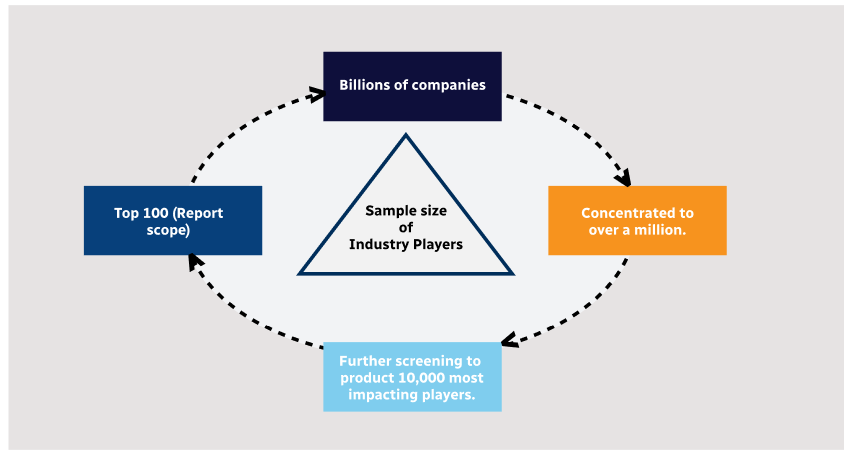
Step 1 - Identification of Relevant Samples Size from Population Database

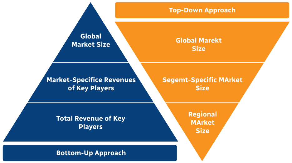
Step 2 - Approaches for Defining Global Market Size (Value, Volume* & Price*)
Note*: In applicable scenarios
Step 3 - Data Sources
Primary Research
- Web Analytics
- Survey Reports
- Research Institute
- Latest Research Reports
- Opinion Leaders
Secondary Research
- Annual Reports
- White Paper
- Latest Press Release
- Industry Association
- Paid Database
- Investor Presentations

Step 4 - Data Triangulation
Involves using different sources of information in order to increase the validity of a study
These sources are likely to be stakeholders in a program - participants, other researchers, program staff, other community members, and so on.
Then we put all data in single framework & apply various statistical tools to find out the dynamic on the market.
During the analysis stage, feedback from the stakeholder groups would be compared to determine areas of agreement as well as areas of divergence