

Key Insights
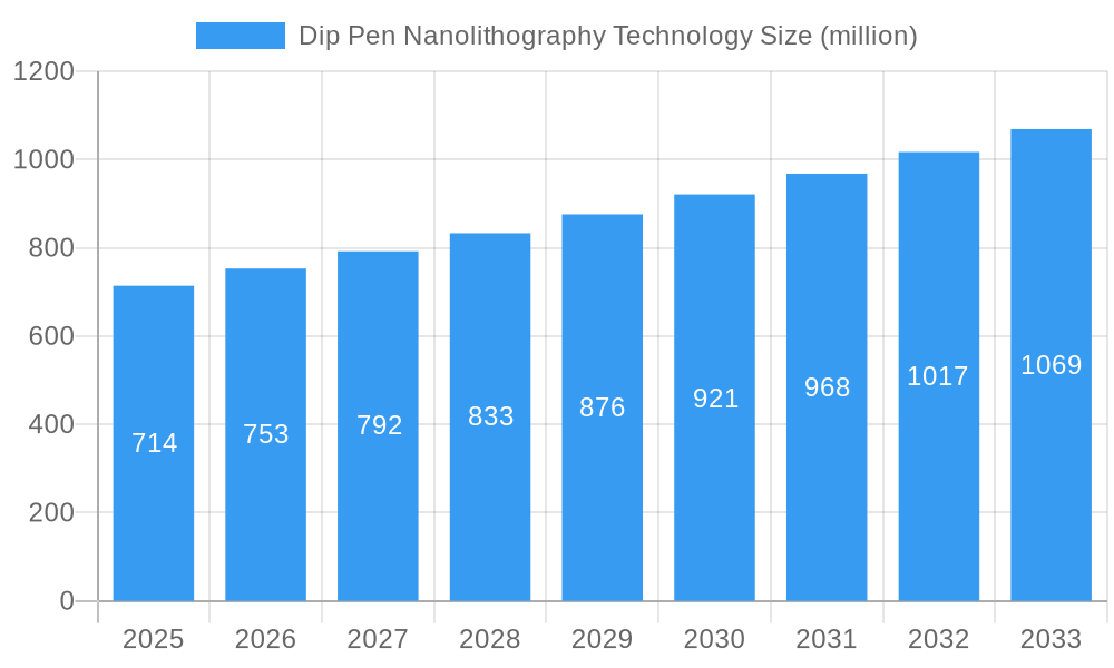
The Dip Pen Nanolithography (DPN) market is poised for significant expansion, projected to reach a substantial size by 2025 and continue its upward trajectory. This growth is fueled by a robust Compound Annual Growth Rate (CAGR) of 5.5%, indicating consistent and strong demand for DPN technologies across various high-impact applications. The market's value is currently estimated at $714 million, a figure expected to increase substantially throughout the forecast period. Key drivers behind this expansion include the burgeoning fields of nano-printing and electrochemical sensing, where DPN's precision and scalability offer unparalleled advantages. Furthermore, advancements in biosensing technologies, driven by the need for highly accurate diagnostics and research tools, are creating new avenues for DPN adoption. The ability of DPN to enable high-resolution pattern printing is also a critical factor, underpinning its utility in the development of next-generation electronic devices, advanced materials, and intricate microfluidic systems.
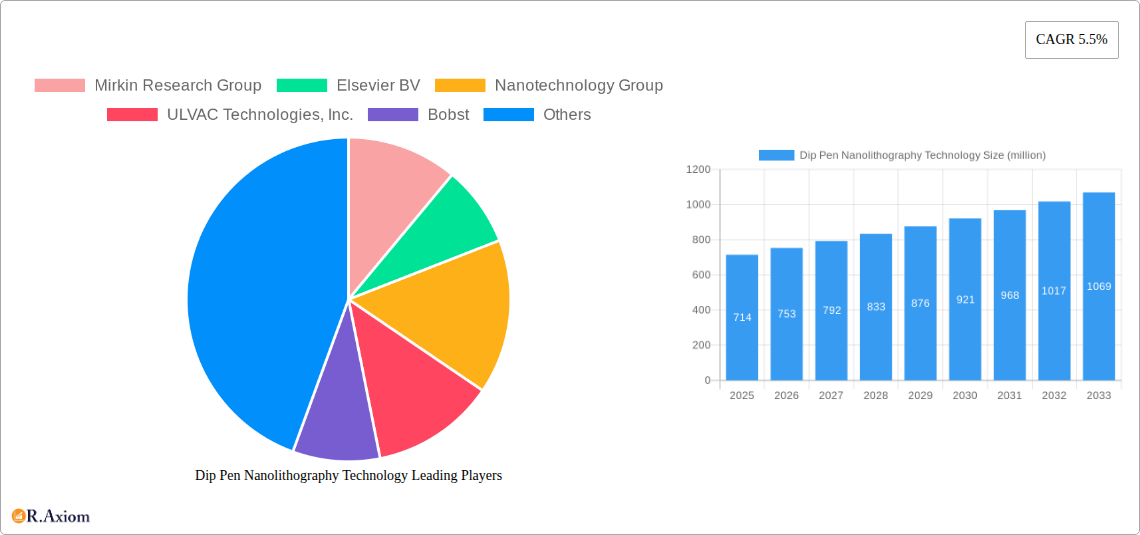
Dip Pen Nanolithography Technology Market Size (In Million)
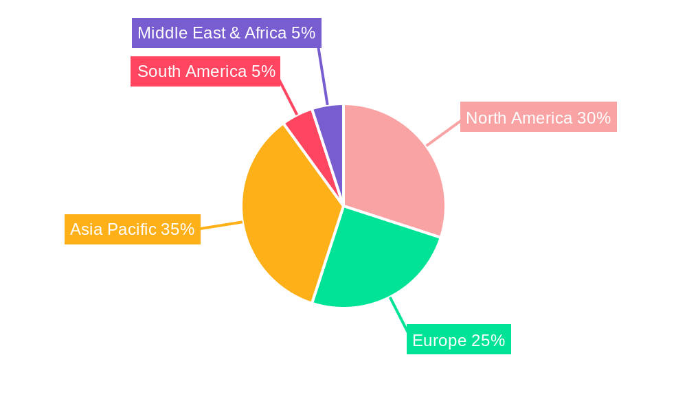
The diverse range of DPN technologies, including Polymer Pen Lithography (PPL), Scanning Probe Block Copolymer Lithography (SPBCL), Beam Pen Lithography (BPL), and Hard Tip-Soft Spring Lithography (HSL), caters to a broad spectrum of industry needs, from academic research to industrial-scale manufacturing. While challenges such as the initial cost of implementation and the need for specialized expertise exist, the overwhelming benefits in terms of resolution, control, and versatility are driving market adoption. Geographically, North America and Asia Pacific are expected to lead the market, owing to strong R&D investments and the presence of key players in the electronics and biotechnology sectors. Europe also presents a significant market, supported by its advanced research infrastructure and growing demand for miniaturized devices. The competitive landscape features a mix of established technology providers and specialized research groups, all contributing to the innovation and growth of the DPN ecosystem.
Dip Pen Nanolithography Technology Company Market Share
Dip Pen Nanolithography Technology Market Concentration & Innovation
The dip pen nanolithography technology market exhibits a moderate to high concentration, with key players such as ULVAC Technologies, Inc., Seiko Epson Corporation, and Canon Inc. investing heavily in research and development. Innovation is primarily driven by the pursuit of ultra-high resolution pattern printing for advanced semiconductor fabrication and the burgeoning demand for miniaturized biosensors in healthcare and diagnostics. Regulatory frameworks, particularly those concerning nanotechnology safety and intellectual property protection, are evolving, influencing R&D trajectories and market entry strategies. Product substitutes, though less precise, include traditional photolithography and electron-beam lithography, which currently hold larger market shares in established applications. End-user trends indicate a strong pull from the electronics industry for next-generation microchips and from the biotechnology sector for personalized medicine and in-vitro diagnostics. Mergers and acquisitions (M&A) are strategically focused on acquiring novel intellectual property and expanding manufacturing capabilities. For instance, recent M&A activities have seen deal values in the hundreds of millions as larger corporations integrate specialized nanolithography expertise. The market share distribution is dynamic, with leading innovators capturing significant portions of niche segments.
- Market Concentration: Moderate to High
- Innovation Drivers: Ultra-high resolution printing, miniaturized biosensors
- Regulatory Influence: Evolving safety standards, IP protection
- Key Product Substitutes: Photolithography, electron-beam lithography
- End-User Trends: Electronics, biotechnology, healthcare
- M&A Activity: Focused on IP acquisition and capability expansion, with deal values in the hundreds of millions.
Dip Pen Nanolithography Technology Industry Trends & Insights
The dip pen nanolithography (DPN) technology landscape is poised for substantial growth, driven by a confluence of technological advancements and escalating demand across diverse sectors. The projected Compound Annual Growth Rate (CAGR) for the DPN market is estimated at an impressive 18.5% over the forecast period of 2025–2033. This robust expansion is fueled by the inherent capabilities of DPN in achieving unparalleled spatial resolution, enabling the precise deposition of various materials at the nanoscale. The nanoprinting application segment, in particular, is experiencing a surge in adoption, driven by the miniaturization trend in consumer electronics and the need for intricate circuitry in next-generation devices. Furthermore, the field of electrochemical sensing and biosensing is a significant growth catalyst. DPN's ability to create highly sensitive and selective sensor arrays for medical diagnostics, environmental monitoring, and food safety applications is opening up vast market opportunities. The penetration of DPN technology in these advanced sensing domains is expected to exceed 30% by 2030, as researchers and commercial entities leverage its precision for developing highly accurate and low-cost diagnostic tools.
Technological disruptions are primarily centered around the development of novel DPN methodologies, such as the refinement of Polymer Pen Lithography (PPL) for large-area patterning and the exploration of Scanning Probe Block Copolymer Lithography (SPBCL) for creating complex nanostructures. The integration of AI and machine learning algorithms into DPN systems is also enhancing control, throughput, and material deposition accuracy, further accelerating market adoption. Consumer preferences are increasingly leaning towards personalized healthcare solutions and advanced functionalities in electronic devices, directly benefiting DPN's ability to create custom-designed nanoscale components and sensors. The competitive dynamics are characterized by a blend of established players with significant R&D investments, such as ULVAC Technologies, Inc. and Seiko Epson Corporation, and agile startups focusing on specialized applications. Strategic partnerships and collaborations are becoming crucial for market players to navigate the complex R&D landscape and accelerate commercialization. The overall market penetration of DPN, though still in its growth phase, is anticipated to reach over 15% across key industrial applications by the end of the forecast period.
Dominant Markets & Segments in Dip Pen Nanolithography Technology
The dip pen nanolithography technology market demonstrates significant dominance in specific regions and application segments, driven by concentrated industrial activity and targeted technological advancements. North America, particularly the United States, and East Asia, encompassing Japan and South Korea, are leading regions. This dominance is underpinned by substantial government investments in nanotechnology research and development, coupled with the presence of leading academic institutions and a robust ecosystem of semiconductor manufacturers and biotechnology firms.
Within the application segments, High Resolution Pattern Printing stands out as the most dominant, directly serving the critical needs of the semiconductor industry for advanced microchip fabrication. The ever-increasing demand for smaller, faster, and more powerful electronic devices necessitates lithography techniques capable of defining features at the sub-10-nanometer scale, a forte of DPN. The market size for this segment alone is projected to reach over $500 million by 2033.
- Key Drivers for High Resolution Pattern Printing Dominance:
- Economic Policies: Government incentives for advanced manufacturing and semiconductor sovereignty initiatives.
- Infrastructure: Presence of world-class semiconductor foundries and research facilities.
- Technological Advancement: Continuous innovation in materials science and precision engineering enabling finer feature definition.
- End-User Demand: Unrelenting consumer and industrial demand for miniaturized and high-performance electronics.
Following closely is the Biosensing application segment, which is experiencing exponential growth. The ability of DPN to create highly precise and multiplexed sensor arrays for diagnostics, drug discovery, and personalized medicine is a significant market driver. The market size for the Biosensing segment is expected to grow at a CAGR of over 20%, reaching approximately $400 million by 2033.
- Key Drivers for Biosensing Dominance:
- Healthcare Advancements: Growing need for early disease detection, point-of-care diagnostics, and targeted therapies.
- Research Funding: Increased allocation of research grants towards life sciences and nanotechnology applications in healthcare.
- Technological Integration: Synergies with microfluidics and lab-on-a-chip technologies.
In terms of technology types, Polymer Pen Lithography (PPL) is currently leading due to its scalability and versatility in depositing a wide range of molecules, making it suitable for both research and emerging industrial applications. Its ability to pattern large areas with high throughput makes it attractive for applications beyond traditional microelectronics.
- Key Drivers for PPL Dominance:
- Scalability: Capable of patterning larger areas compared to some other SPM-based techniques.
- Material Versatility: Ability to deposit diverse materials, including biomolecules, nanoparticles, and polymers.
- Cost-Effectiveness: Potentially lower cost for large-area patterning compared to some extreme ultraviolet lithography (EUV) methods for specific applications.
The Electrochemical Sensing segment also shows considerable promise, driven by the demand for portable and low-cost sensors for environmental monitoring, industrial process control, and wearable health devices. High Resolution Pattern Printing is a cornerstone technology, directly impacting the advancements within these sensing applications. The interplay between these segments highlights the broad and impactful reach of dip pen nanolithography.
Dip Pen Nanolithography Technology Product Developments
Product developments in dip pen nanolithography technology are characterized by advancements in resolution, material compatibility, and throughput. Innovations are focused on enabling the precise deposition of novel materials, including quantum dots and advanced polymers, for applications in next-generation displays, solar cells, and integrated circuits. The development of more robust and versatile pen arrays, capable of simultaneous patterning, significantly enhances manufacturing efficiency. Competitive advantages are being gained through increased process speed, reduced defect rates, and the ability to create complex 3D nanostructures. These technological trends are directly addressing the market's demand for faster, more reliable, and cost-effective nanoscale fabrication solutions, opening doors for expanded adoption in diverse industrial sectors.
Report Scope & Segmentation Analysis
This report provides a comprehensive analysis of the dip pen nanolithography technology market, encompassing key segments. The Application segments analyzed include Nano Printing, crucial for advanced manufacturing and electronics; Electrochemical Sensing, vital for diagnostics and environmental monitoring; Biosensing, pivotal for healthcare and life sciences; and High Resolution Pattern Printing, the bedrock of semiconductor innovation. The Type segments covered are Polymer Pen Lithography (PPL), known for its versatility; Scanning Probe Block Copolymer Lithography (SPBCL), enabling intricate nanostructure formation; Beam Pen Lithography (BPL), offering unique material deposition capabilities; and Hard Tip-Soft Spring Lithography (HSL), focused on precise patterning with reduced substrate damage. Projections indicate robust growth across all segments, with Nano Printing and High Resolution Pattern Printing anticipated to lead in market size, reaching estimated values of over $700 million and over $500 million respectively by 2033.
- Nano Printing: Expected CAGR of over 19%, market size projected to reach over $700 million by 2033.
- Electrochemical Sensing: Expected CAGR of over 17%, market size projected to reach over $350 million by 2033.
- Biosensing: Expected CAGR of over 20%, market size projected to reach over $400 million by 2033.
- High Resolution Pattern Printing: Expected CAGR of over 18%, market size projected to reach over $500 million by 2033.
- Polymer Pen Lithography (PPL): Dominant type, projected to capture over 40% of the type segment market share.
- Scanning Probe Block Copolymer Lithography (SPBCL): Niche but growing, with projected market size of over $150 million by 2033.
- Beam Pen Lithography (BPL): Specialized applications, projected market size of over $100 million by 2033.
- Hard Tip-Soft Spring Lithography (HSL): Emerging technology with significant potential, projected market size of over $80 million by 2033.
Key Drivers of Dip Pen Nanolithography Technology Growth
The growth of the dip pen nanolithography technology market is propelled by several interconnected factors. The relentless demand for miniaturization and increased functionality in the electronics sector, particularly in semiconductors and advanced displays, is a primary driver. Government initiatives worldwide promoting nanotechnology research and its commercialization, coupled with substantial funding for R&D in areas like quantum computing and advanced materials, further fuel expansion. The burgeoning healthcare industry's need for highly sensitive and precise diagnostic tools, especially in the realm of biosensing and personalized medicine, presents a significant growth avenue. Furthermore, the continuous innovation in DPN methodologies, leading to higher resolution, faster patterning speeds, and broader material compatibility, is enhancing its attractiveness for industrial adoption.
- Technological Advancements: Improved resolution, throughput, and material versatility.
- Market Demand: Miniaturization in electronics, advanced diagnostics in healthcare.
- Government Support: R&D funding, strategic initiatives for nanotechnology commercialization.
- Academic Research: Breakthroughs in materials science and fabrication techniques.
Challenges in the Dip Pen Nanolithography Technology Sector
Despite its promising trajectory, the dip pen nanolithography technology sector faces several challenges. The high cost of sophisticated equipment and materials can be a significant barrier to widespread adoption, especially for smaller enterprises. Scaling up DPN processes from laboratory settings to mass production remains a technical hurdle, impacting throughput and consistency. Furthermore, the regulatory landscape for nanotechnology applications, particularly concerning safety and environmental impact, is still evolving, creating uncertainty for market players. The availability of skilled personnel with expertise in nanoscale fabrication and DPN operation is also a constraint. Competitive pressures from established lithography techniques, which possess mature supply chains and infrastructure, necessitate continuous innovation and cost optimization for DPN to gain market share.
- Cost of Equipment and Materials: High initial investment.
- Scalability Issues: Transitioning from lab to mass production.
- Evolving Regulatory Frameworks: Uncertainty regarding safety and environmental standards.
- Talent Shortage: Lack of highly skilled DPN operators and researchers.
- Competition from Established Technologies: Mature infrastructure of traditional lithography.
Emerging Opportunities in Dip Pen Nanolithography Technology
Emerging opportunities in the dip pen nanolithography technology sector are diverse and represent significant growth potential. The development of novel DPN applications in the field of additive manufacturing for micro- and nano-scale components is a key area. The integration of DPN with artificial intelligence and machine learning is enabling more sophisticated and autonomous patterning processes, opening doors for advanced materials design and fabrication. The increasing demand for flexible electronics and wearable devices presents a substantial market for DPN's ability to pattern on diverse substrates. Furthermore, the exploration of DPN for creating quantum computing components and advanced sensor networks for the Internet of Things (IoT) devices offers promising future avenues.
- Additive Manufacturing: Micro- and nano-scale 3D printing.
- AI Integration: Autonomous patterning and materials design.
- Flexible Electronics: Patterning on unconventional substrates.
- Quantum Computing: Fabrication of novel quantum devices.
- IoT Sensors: Development of miniaturized and integrated sensing solutions.
Leading Players in the Dip Pen Nanolithography Technology Market
- Mirkin Research Group
- Elsevier BV
- Nanotechnology Group
- ULVAC Technologies, Inc.
- Bobst
- Brother Industries
- KOMORI Corporation
- Seiko Epson Corporation
- SPGPrints BV
- Meyer Burger
- Methode Electronics
- KONICA MINOLTA
- Koenig & Bauer
- Xerox Corporation.
- Canon Inc.
- SCREEN Holdings
Key Developments in Dip Pen Nanolithography Technology Industry
- 2019: Advancement in Polymer Pen Lithography (PPL) enabling high-throughput patterning of biomolecules for drug delivery research.
- 2020: Development of novel ink formulations for DPN, expanding material compatibility for semiconductor applications.
- 2021: Introduction of automated DPN systems with enhanced precision for large-area fabrication in industrial settings.
- 2022: Breakthrough in Scanning Probe Block Copolymer Lithography (SPBCL) for creating complex 3D nanostructures with sub-10nm resolution.
- 2023: Integration of machine learning algorithms into DPN control systems for predictive maintenance and optimized deposition.
- 2024: Significant increase in R&D investment from major corporations like Seiko Epson Corporation and Canon Inc. in the DPN sector.
Strategic Outlook for Dip Pen Nanolithography Technology Market
The strategic outlook for the dip pen nanolithography technology market is overwhelmingly positive, characterized by sustained innovation and expanding application horizons. Growth catalysts include the continued miniaturization trend in electronics, the rapidly evolving healthcare sector's demand for advanced diagnostics, and the increasing governmental support for nanotechnology research. The ability of DPN to offer unparalleled precision, versatility in material deposition, and potential for cost-effective large-area patterning positions it as a critical technology for future advancements in semiconductor manufacturing, advanced sensing, and novel materials development. Strategic collaborations between research institutions and industry players, coupled with ongoing advancements in DPN hardware and software, will be crucial for overcoming existing challenges and unlocking the full market potential, projecting a market value estimated to exceed $3 billion by 2033.
Dip Pen Nanolithography Technology Segmentation
-
1. Application
- 1.1. Nano Printing
- 1.2. Electrochemical Sensing
- 1.3. Biosensing
- 1.4. High Resolution Pattern Printing
-
2. Type
- 2.1. Polymer Pen Lithography (PPL)
- 2.2. Scanning Probe Block Copolymer Lithography (SPBCL)
- 2.3. Beam Pen Lithography (BPL)
- 2.4. Hard Tip-Soft Spring Lithography (HSL)
Dip Pen Nanolithography Technology Segmentation By Geography
-
1. North America
- 1.1. United States
- 1.2. Canada
- 1.3. Mexico
-
2. South America
- 2.1. Brazil
- 2.2. Argentina
- 2.3. Rest of South America
-
3. Europe
- 3.1. United Kingdom
- 3.2. Germany
- 3.3. France
- 3.4. Italy
- 3.5. Spain
- 3.6. Russia
- 3.7. Benelux
- 3.8. Nordics
- 3.9. Rest of Europe
-
4. Middle East & Africa
- 4.1. Turkey
- 4.2. Israel
- 4.3. GCC
- 4.4. North Africa
- 4.5. South Africa
- 4.6. Rest of Middle East & Africa
-
5. Asia Pacific
- 5.1. China
- 5.2. India
- 5.3. Japan
- 5.4. South Korea
- 5.5. ASEAN
- 5.6. Oceania
- 5.7. Rest of Asia Pacific
Dip Pen Nanolithography Technology Regional Market Share
Geographic Coverage of Dip Pen Nanolithography Technology
Dip Pen Nanolithography Technology REPORT HIGHLIGHTS
| Aspects | Details |
|---|---|
| Study Period | 2020-2034 |
| Base Year | 2025 |
| Estimated Year | 2026 |
| Forecast Period | 2026-2034 |
| Historical Period | 2020-2025 |
| Growth Rate | CAGR of 5.5% from 2020-2034 |
| Segmentation |
|
Table of Contents
- 1. Introduction
- 1.1. Research Scope
- 1.2. Market Segmentation
- 1.3. Research Methodology
- 1.4. Definitions and Assumptions
- 2. Executive Summary
- 2.1. Introduction
- 3. Market Dynamics
- 3.1. Introduction
- 3.2. Market Drivers
- 3.3. Market Restrains
- 3.4. Market Trends
- 4. Market Factor Analysis
- 4.1. Porters Five Forces
- 4.2. Supply/Value Chain
- 4.3. PESTEL analysis
- 4.4. Market Entropy
- 4.5. Patent/Trademark Analysis
- 5. Global Dip Pen Nanolithography Technology Analysis, Insights and Forecast, 2020-2032
- 5.1. Market Analysis, Insights and Forecast - by Application
- 5.1.1. Nano Printing
- 5.1.2. Electrochemical Sensing
- 5.1.3. Biosensing
- 5.1.4. High Resolution Pattern Printing
- 5.2. Market Analysis, Insights and Forecast - by Type
- 5.2.1. Polymer Pen Lithography (PPL)
- 5.2.2. Scanning Probe Block Copolymer Lithography (SPBCL)
- 5.2.3. Beam Pen Lithography (BPL)
- 5.2.4. Hard Tip-Soft Spring Lithography (HSL)
- 5.3. Market Analysis, Insights and Forecast - by Region
- 5.3.1. North America
- 5.3.2. South America
- 5.3.3. Europe
- 5.3.4. Middle East & Africa
- 5.3.5. Asia Pacific
- 5.1. Market Analysis, Insights and Forecast - by Application
- 6. North America Dip Pen Nanolithography Technology Analysis, Insights and Forecast, 2020-2032
- 6.1. Market Analysis, Insights and Forecast - by Application
- 6.1.1. Nano Printing
- 6.1.2. Electrochemical Sensing
- 6.1.3. Biosensing
- 6.1.4. High Resolution Pattern Printing
- 6.2. Market Analysis, Insights and Forecast - by Type
- 6.2.1. Polymer Pen Lithography (PPL)
- 6.2.2. Scanning Probe Block Copolymer Lithography (SPBCL)
- 6.2.3. Beam Pen Lithography (BPL)
- 6.2.4. Hard Tip-Soft Spring Lithography (HSL)
- 6.1. Market Analysis, Insights and Forecast - by Application
- 7. South America Dip Pen Nanolithography Technology Analysis, Insights and Forecast, 2020-2032
- 7.1. Market Analysis, Insights and Forecast - by Application
- 7.1.1. Nano Printing
- 7.1.2. Electrochemical Sensing
- 7.1.3. Biosensing
- 7.1.4. High Resolution Pattern Printing
- 7.2. Market Analysis, Insights and Forecast - by Type
- 7.2.1. Polymer Pen Lithography (PPL)
- 7.2.2. Scanning Probe Block Copolymer Lithography (SPBCL)
- 7.2.3. Beam Pen Lithography (BPL)
- 7.2.4. Hard Tip-Soft Spring Lithography (HSL)
- 7.1. Market Analysis, Insights and Forecast - by Application
- 8. Europe Dip Pen Nanolithography Technology Analysis, Insights and Forecast, 2020-2032
- 8.1. Market Analysis, Insights and Forecast - by Application
- 8.1.1. Nano Printing
- 8.1.2. Electrochemical Sensing
- 8.1.3. Biosensing
- 8.1.4. High Resolution Pattern Printing
- 8.2. Market Analysis, Insights and Forecast - by Type
- 8.2.1. Polymer Pen Lithography (PPL)
- 8.2.2. Scanning Probe Block Copolymer Lithography (SPBCL)
- 8.2.3. Beam Pen Lithography (BPL)
- 8.2.4. Hard Tip-Soft Spring Lithography (HSL)
- 8.1. Market Analysis, Insights and Forecast - by Application
- 9. Middle East & Africa Dip Pen Nanolithography Technology Analysis, Insights and Forecast, 2020-2032
- 9.1. Market Analysis, Insights and Forecast - by Application
- 9.1.1. Nano Printing
- 9.1.2. Electrochemical Sensing
- 9.1.3. Biosensing
- 9.1.4. High Resolution Pattern Printing
- 9.2. Market Analysis, Insights and Forecast - by Type
- 9.2.1. Polymer Pen Lithography (PPL)
- 9.2.2. Scanning Probe Block Copolymer Lithography (SPBCL)
- 9.2.3. Beam Pen Lithography (BPL)
- 9.2.4. Hard Tip-Soft Spring Lithography (HSL)
- 9.1. Market Analysis, Insights and Forecast - by Application
- 10. Asia Pacific Dip Pen Nanolithography Technology Analysis, Insights and Forecast, 2020-2032
- 10.1. Market Analysis, Insights and Forecast - by Application
- 10.1.1. Nano Printing
- 10.1.2. Electrochemical Sensing
- 10.1.3. Biosensing
- 10.1.4. High Resolution Pattern Printing
- 10.2. Market Analysis, Insights and Forecast - by Type
- 10.2.1. Polymer Pen Lithography (PPL)
- 10.2.2. Scanning Probe Block Copolymer Lithography (SPBCL)
- 10.2.3. Beam Pen Lithography (BPL)
- 10.2.4. Hard Tip-Soft Spring Lithography (HSL)
- 10.1. Market Analysis, Insights and Forecast - by Application
- 11. Competitive Analysis
- 11.1. Global Market Share Analysis 2025
- 11.2. Company Profiles
- 11.2.1 Mirkin Research Group
- 11.2.1.1. Overview
- 11.2.1.2. Products
- 11.2.1.3. SWOT Analysis
- 11.2.1.4. Recent Developments
- 11.2.1.5. Financials (Based on Availability)
- 11.2.2 Elsevier BV
- 11.2.2.1. Overview
- 11.2.2.2. Products
- 11.2.2.3. SWOT Analysis
- 11.2.2.4. Recent Developments
- 11.2.2.5. Financials (Based on Availability)
- 11.2.3 Nanotechnology Group
- 11.2.3.1. Overview
- 11.2.3.2. Products
- 11.2.3.3. SWOT Analysis
- 11.2.3.4. Recent Developments
- 11.2.3.5. Financials (Based on Availability)
- 11.2.4 ULVAC Technologies Inc.
- 11.2.4.1. Overview
- 11.2.4.2. Products
- 11.2.4.3. SWOT Analysis
- 11.2.4.4. Recent Developments
- 11.2.4.5. Financials (Based on Availability)
- 11.2.5 Bobst
- 11.2.5.1. Overview
- 11.2.5.2. Products
- 11.2.5.3. SWOT Analysis
- 11.2.5.4. Recent Developments
- 11.2.5.5. Financials (Based on Availability)
- 11.2.6 Brother Industries
- 11.2.6.1. Overview
- 11.2.6.2. Products
- 11.2.6.3. SWOT Analysis
- 11.2.6.4. Recent Developments
- 11.2.6.5. Financials (Based on Availability)
- 11.2.7 KOMORI Corporation
- 11.2.7.1. Overview
- 11.2.7.2. Products
- 11.2.7.3. SWOT Analysis
- 11.2.7.4. Recent Developments
- 11.2.7.5. Financials (Based on Availability)
- 11.2.8 Seiko Epson Corporation
- 11.2.8.1. Overview
- 11.2.8.2. Products
- 11.2.8.3. SWOT Analysis
- 11.2.8.4. Recent Developments
- 11.2.8.5. Financials (Based on Availability)
- 11.2.9 SPGPrints BV
- 11.2.9.1. Overview
- 11.2.9.2. Products
- 11.2.9.3. SWOT Analysis
- 11.2.9.4. Recent Developments
- 11.2.9.5. Financials (Based on Availability)
- 11.2.10 Meyer Burger
- 11.2.10.1. Overview
- 11.2.10.2. Products
- 11.2.10.3. SWOT Analysis
- 11.2.10.4. Recent Developments
- 11.2.10.5. Financials (Based on Availability)
- 11.2.11 Methode Electronics
- 11.2.11.1. Overview
- 11.2.11.2. Products
- 11.2.11.3. SWOT Analysis
- 11.2.11.4. Recent Developments
- 11.2.11.5. Financials (Based on Availability)
- 11.2.12 KONICA MINOLTA
- 11.2.12.1. Overview
- 11.2.12.2. Products
- 11.2.12.3. SWOT Analysis
- 11.2.12.4. Recent Developments
- 11.2.12.5. Financials (Based on Availability)
- 11.2.13 Koenig & Bauer
- 11.2.13.1. Overview
- 11.2.13.2. Products
- 11.2.13.3. SWOT Analysis
- 11.2.13.4. Recent Developments
- 11.2.13.5. Financials (Based on Availability)
- 11.2.14 Xerox Corporation.
- 11.2.14.1. Overview
- 11.2.14.2. Products
- 11.2.14.3. SWOT Analysis
- 11.2.14.4. Recent Developments
- 11.2.14.5. Financials (Based on Availability)
- 11.2.15 Canon Inc.
- 11.2.15.1. Overview
- 11.2.15.2. Products
- 11.2.15.3. SWOT Analysis
- 11.2.15.4. Recent Developments
- 11.2.15.5. Financials (Based on Availability)
- 11.2.16 SCREEN Holdings
- 11.2.16.1. Overview
- 11.2.16.2. Products
- 11.2.16.3. SWOT Analysis
- 11.2.16.4. Recent Developments
- 11.2.16.5. Financials (Based on Availability)
- 11.2.1 Mirkin Research Group
List of Figures
- Figure 1: Global Dip Pen Nanolithography Technology Revenue Breakdown (million, %) by Region 2025 & 2033
- Figure 2: North America Dip Pen Nanolithography Technology Revenue (million), by Application 2025 & 2033
- Figure 3: North America Dip Pen Nanolithography Technology Revenue Share (%), by Application 2025 & 2033
- Figure 4: North America Dip Pen Nanolithography Technology Revenue (million), by Type 2025 & 2033
- Figure 5: North America Dip Pen Nanolithography Technology Revenue Share (%), by Type 2025 & 2033
- Figure 6: North America Dip Pen Nanolithography Technology Revenue (million), by Country 2025 & 2033
- Figure 7: North America Dip Pen Nanolithography Technology Revenue Share (%), by Country 2025 & 2033
- Figure 8: South America Dip Pen Nanolithography Technology Revenue (million), by Application 2025 & 2033
- Figure 9: South America Dip Pen Nanolithography Technology Revenue Share (%), by Application 2025 & 2033
- Figure 10: South America Dip Pen Nanolithography Technology Revenue (million), by Type 2025 & 2033
- Figure 11: South America Dip Pen Nanolithography Technology Revenue Share (%), by Type 2025 & 2033
- Figure 12: South America Dip Pen Nanolithography Technology Revenue (million), by Country 2025 & 2033
- Figure 13: South America Dip Pen Nanolithography Technology Revenue Share (%), by Country 2025 & 2033
- Figure 14: Europe Dip Pen Nanolithography Technology Revenue (million), by Application 2025 & 2033
- Figure 15: Europe Dip Pen Nanolithography Technology Revenue Share (%), by Application 2025 & 2033
- Figure 16: Europe Dip Pen Nanolithography Technology Revenue (million), by Type 2025 & 2033
- Figure 17: Europe Dip Pen Nanolithography Technology Revenue Share (%), by Type 2025 & 2033
- Figure 18: Europe Dip Pen Nanolithography Technology Revenue (million), by Country 2025 & 2033
- Figure 19: Europe Dip Pen Nanolithography Technology Revenue Share (%), by Country 2025 & 2033
- Figure 20: Middle East & Africa Dip Pen Nanolithography Technology Revenue (million), by Application 2025 & 2033
- Figure 21: Middle East & Africa Dip Pen Nanolithography Technology Revenue Share (%), by Application 2025 & 2033
- Figure 22: Middle East & Africa Dip Pen Nanolithography Technology Revenue (million), by Type 2025 & 2033
- Figure 23: Middle East & Africa Dip Pen Nanolithography Technology Revenue Share (%), by Type 2025 & 2033
- Figure 24: Middle East & Africa Dip Pen Nanolithography Technology Revenue (million), by Country 2025 & 2033
- Figure 25: Middle East & Africa Dip Pen Nanolithography Technology Revenue Share (%), by Country 2025 & 2033
- Figure 26: Asia Pacific Dip Pen Nanolithography Technology Revenue (million), by Application 2025 & 2033
- Figure 27: Asia Pacific Dip Pen Nanolithography Technology Revenue Share (%), by Application 2025 & 2033
- Figure 28: Asia Pacific Dip Pen Nanolithography Technology Revenue (million), by Type 2025 & 2033
- Figure 29: Asia Pacific Dip Pen Nanolithography Technology Revenue Share (%), by Type 2025 & 2033
- Figure 30: Asia Pacific Dip Pen Nanolithography Technology Revenue (million), by Country 2025 & 2033
- Figure 31: Asia Pacific Dip Pen Nanolithography Technology Revenue Share (%), by Country 2025 & 2033
List of Tables
- Table 1: Global Dip Pen Nanolithography Technology Revenue million Forecast, by Application 2020 & 2033
- Table 2: Global Dip Pen Nanolithography Technology Revenue million Forecast, by Type 2020 & 2033
- Table 3: Global Dip Pen Nanolithography Technology Revenue million Forecast, by Region 2020 & 2033
- Table 4: Global Dip Pen Nanolithography Technology Revenue million Forecast, by Application 2020 & 2033
- Table 5: Global Dip Pen Nanolithography Technology Revenue million Forecast, by Type 2020 & 2033
- Table 6: Global Dip Pen Nanolithography Technology Revenue million Forecast, by Country 2020 & 2033
- Table 7: United States Dip Pen Nanolithography Technology Revenue (million) Forecast, by Application 2020 & 2033
- Table 8: Canada Dip Pen Nanolithography Technology Revenue (million) Forecast, by Application 2020 & 2033
- Table 9: Mexico Dip Pen Nanolithography Technology Revenue (million) Forecast, by Application 2020 & 2033
- Table 10: Global Dip Pen Nanolithography Technology Revenue million Forecast, by Application 2020 & 2033
- Table 11: Global Dip Pen Nanolithography Technology Revenue million Forecast, by Type 2020 & 2033
- Table 12: Global Dip Pen Nanolithography Technology Revenue million Forecast, by Country 2020 & 2033
- Table 13: Brazil Dip Pen Nanolithography Technology Revenue (million) Forecast, by Application 2020 & 2033
- Table 14: Argentina Dip Pen Nanolithography Technology Revenue (million) Forecast, by Application 2020 & 2033
- Table 15: Rest of South America Dip Pen Nanolithography Technology Revenue (million) Forecast, by Application 2020 & 2033
- Table 16: Global Dip Pen Nanolithography Technology Revenue million Forecast, by Application 2020 & 2033
- Table 17: Global Dip Pen Nanolithography Technology Revenue million Forecast, by Type 2020 & 2033
- Table 18: Global Dip Pen Nanolithography Technology Revenue million Forecast, by Country 2020 & 2033
- Table 19: United Kingdom Dip Pen Nanolithography Technology Revenue (million) Forecast, by Application 2020 & 2033
- Table 20: Germany Dip Pen Nanolithography Technology Revenue (million) Forecast, by Application 2020 & 2033
- Table 21: France Dip Pen Nanolithography Technology Revenue (million) Forecast, by Application 2020 & 2033
- Table 22: Italy Dip Pen Nanolithography Technology Revenue (million) Forecast, by Application 2020 & 2033
- Table 23: Spain Dip Pen Nanolithography Technology Revenue (million) Forecast, by Application 2020 & 2033
- Table 24: Russia Dip Pen Nanolithography Technology Revenue (million) Forecast, by Application 2020 & 2033
- Table 25: Benelux Dip Pen Nanolithography Technology Revenue (million) Forecast, by Application 2020 & 2033
- Table 26: Nordics Dip Pen Nanolithography Technology Revenue (million) Forecast, by Application 2020 & 2033
- Table 27: Rest of Europe Dip Pen Nanolithography Technology Revenue (million) Forecast, by Application 2020 & 2033
- Table 28: Global Dip Pen Nanolithography Technology Revenue million Forecast, by Application 2020 & 2033
- Table 29: Global Dip Pen Nanolithography Technology Revenue million Forecast, by Type 2020 & 2033
- Table 30: Global Dip Pen Nanolithography Technology Revenue million Forecast, by Country 2020 & 2033
- Table 31: Turkey Dip Pen Nanolithography Technology Revenue (million) Forecast, by Application 2020 & 2033
- Table 32: Israel Dip Pen Nanolithography Technology Revenue (million) Forecast, by Application 2020 & 2033
- Table 33: GCC Dip Pen Nanolithography Technology Revenue (million) Forecast, by Application 2020 & 2033
- Table 34: North Africa Dip Pen Nanolithography Technology Revenue (million) Forecast, by Application 2020 & 2033
- Table 35: South Africa Dip Pen Nanolithography Technology Revenue (million) Forecast, by Application 2020 & 2033
- Table 36: Rest of Middle East & Africa Dip Pen Nanolithography Technology Revenue (million) Forecast, by Application 2020 & 2033
- Table 37: Global Dip Pen Nanolithography Technology Revenue million Forecast, by Application 2020 & 2033
- Table 38: Global Dip Pen Nanolithography Technology Revenue million Forecast, by Type 2020 & 2033
- Table 39: Global Dip Pen Nanolithography Technology Revenue million Forecast, by Country 2020 & 2033
- Table 40: China Dip Pen Nanolithography Technology Revenue (million) Forecast, by Application 2020 & 2033
- Table 41: India Dip Pen Nanolithography Technology Revenue (million) Forecast, by Application 2020 & 2033
- Table 42: Japan Dip Pen Nanolithography Technology Revenue (million) Forecast, by Application 2020 & 2033
- Table 43: South Korea Dip Pen Nanolithography Technology Revenue (million) Forecast, by Application 2020 & 2033
- Table 44: ASEAN Dip Pen Nanolithography Technology Revenue (million) Forecast, by Application 2020 & 2033
- Table 45: Oceania Dip Pen Nanolithography Technology Revenue (million) Forecast, by Application 2020 & 2033
- Table 46: Rest of Asia Pacific Dip Pen Nanolithography Technology Revenue (million) Forecast, by Application 2020 & 2033
Frequently Asked Questions
1. What is the projected Compound Annual Growth Rate (CAGR) of the Dip Pen Nanolithography Technology?
The projected CAGR is approximately 5.5%.
2. Which companies are prominent players in the Dip Pen Nanolithography Technology?
Key companies in the market include Mirkin Research Group, Elsevier BV, Nanotechnology Group, ULVAC Technologies, Inc., Bobst, Brother Industries, KOMORI Corporation, Seiko Epson Corporation, SPGPrints BV, Meyer Burger, Methode Electronics, KONICA MINOLTA, Koenig & Bauer, Xerox Corporation., Canon Inc., SCREEN Holdings.
3. What are the main segments of the Dip Pen Nanolithography Technology?
The market segments include Application, Type.
4. Can you provide details about the market size?
The market size is estimated to be USD 714 million as of 2022.
5. What are some drivers contributing to market growth?
N/A
6. What are the notable trends driving market growth?
N/A
7. Are there any restraints impacting market growth?
N/A
8. Can you provide examples of recent developments in the market?
N/A
9. What pricing options are available for accessing the report?
Pricing options include single-user, multi-user, and enterprise licenses priced at USD 2900.00, USD 4350.00, and USD 5800.00 respectively.
10. Is the market size provided in terms of value or volume?
The market size is provided in terms of value, measured in million.
11. Are there any specific market keywords associated with the report?
Yes, the market keyword associated with the report is "Dip Pen Nanolithography Technology," which aids in identifying and referencing the specific market segment covered.
12. How do I determine which pricing option suits my needs best?
The pricing options vary based on user requirements and access needs. Individual users may opt for single-user licenses, while businesses requiring broader access may choose multi-user or enterprise licenses for cost-effective access to the report.
13. Are there any additional resources or data provided in the Dip Pen Nanolithography Technology report?
While the report offers comprehensive insights, it's advisable to review the specific contents or supplementary materials provided to ascertain if additional resources or data are available.
14. How can I stay updated on further developments or reports in the Dip Pen Nanolithography Technology?
To stay informed about further developments, trends, and reports in the Dip Pen Nanolithography Technology, consider subscribing to industry newsletters, following relevant companies and organizations, or regularly checking reputable industry news sources and publications.
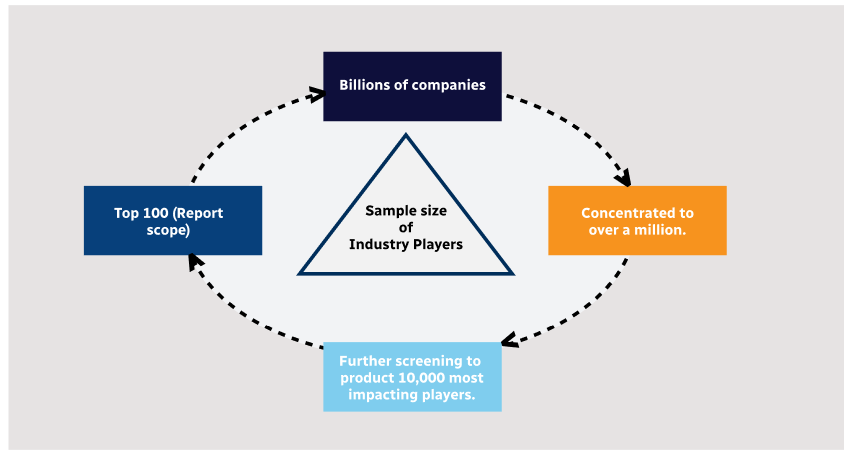
Methodology
Step 1 - Identification of Relevant Samples Size from Population Database

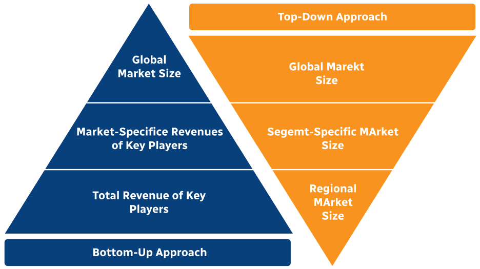
Step 2 - Approaches for Defining Global Market Size (Value, Volume* & Price*)
Note*: In applicable scenarios
Step 3 - Data Sources
Primary Research
- Web Analytics
- Survey Reports
- Research Institute
- Latest Research Reports
- Opinion Leaders
Secondary Research
- Annual Reports
- White Paper
- Latest Press Release
- Industry Association
- Paid Database
- Investor Presentations

Step 4 - Data Triangulation
Involves using different sources of information in order to increase the validity of a study
These sources are likely to be stakeholders in a program - participants, other researchers, program staff, other community members, and so on.
Then we put all data in single framework & apply various statistical tools to find out the dynamic on the market.
During the analysis stage, feedback from the stakeholder groups would be compared to determine areas of agreement as well as areas of divergence