
Key Insights
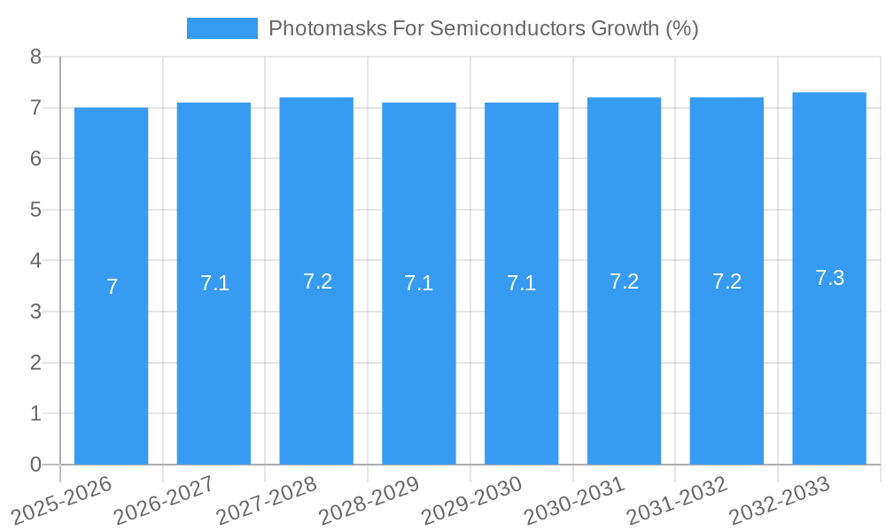
The global Photomasks for Semiconductors market is poised for significant expansion, projected to reach approximately USD 5,000 million by 2025 and exhibiting a Compound Annual Growth Rate (CAGR) of around 7% through 2033. This robust growth is underpinned by escalating demand across critical sectors, with Consumer Electronics leading the charge, followed closely by the Automobile and Telecommunication industries. The increasing sophistication and miniaturization of electronic components in smartphones, wearables, and advanced computing systems are directly fueling the need for high-precision photomasks. Furthermore, the burgeoning automotive sector, with its rapid adoption of electric vehicles (EVs) and advanced driver-assistance systems (ADAS), requires a greater number of specialized semiconductors, thus driving photomask production. The Telecommunication industry's ongoing 5G rollout and the subsequent demand for enhanced network infrastructure also represent a substantial growth avenue. Medical devices and the Internet of Things (IoT) ecosystem, while currently smaller segments, are expected to contribute to sustained market expansion due to their inherent reliance on microelectronic components.
Key market drivers include continuous innovation in semiconductor manufacturing processes, necessitating increasingly complex and high-resolution photomasks, and the growing adoption of advanced packaging techniques. The trend towards smaller feature sizes in integrated circuits (ICs) directly translates to a demand for more intricate and accurate photomasks, pushing technological boundaries. However, the market faces certain restraints, notably the high capital expenditure required for advanced photomask manufacturing facilities and the prolonged lead times associated with producing highly specialized masks. Geographically, Asia Pacific, particularly China, Japan, and South Korea, is expected to dominate the market share due to its established semiconductor manufacturing ecosystem and significant production capabilities. North America and Europe also hold substantial market presence, driven by their advanced research and development capabilities and burgeoning application sectors like automotive and medical. The market segmentation by type reveals a strong demand for Binary Photomasks due to their widespread application in current manufacturing processes, alongside a growing interest in Phase Shifting Masks for advanced node manufacturing.
Photomasks For Semiconductors Market: Comprehensive Analysis & Forecast (2019-2033)
This in-depth report provides a comprehensive analysis of the global photomasks for semiconductors market. Covering the historical period from 2019 to 2024, the base year of 2025, and a detailed forecast period extending to 2033, this report offers critical insights into market dynamics, key players, emerging trends, and future growth opportunities. With a focus on high-traffic keywords such as "semiconductor photomasks," "photomask manufacturing," "advanced lithography," and "semiconductor industry trends," this report is designed to be an indispensable resource for industry stakeholders, investors, and researchers seeking to understand the evolving landscape of semiconductor photomask production and its vital role in enabling advanced electronic devices.
Photomasks For Semiconductors Market Concentration & Innovation
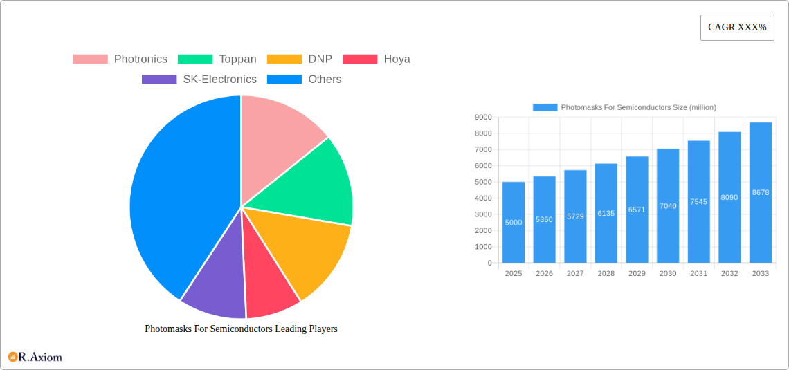
The global photomasks for semiconductors market exhibits a moderate to high level of concentration, with leading players like Photronics, Toppan, and DNP holding significant market share, estimated in the range of tens of billions of dollars in annual revenue. Innovation remains a key differentiator, driven by the relentless demand for smaller feature sizes and higher performance in semiconductor devices. Companies are heavily investing in research and development for advanced photomask technologies, including EUV (Extreme Ultraviolet) photomasks and multi-patterning techniques. Regulatory frameworks, while generally supportive of technological advancement, focus on intellectual property protection and supply chain security. Product substitutes are limited due to the highly specialized nature of photomasks, though advancements in direct-write lithography could pose a long-term challenge. End-user trends, particularly the insatiable demand from consumer electronics, automotive, and telecommunications sectors, are primary innovation drivers. Mergers and acquisitions (M&A) activity, while not overtly frequent, often involves strategic consolidations or technology acquisitions, with deal values potentially reaching hundreds of millions of dollars for specialized capabilities.
Photomasks For Semiconductors Industry Trends & Insights
The photomasks for semiconductors industry is experiencing robust growth, projected to achieve a Compound Annual Growth Rate (CAGR) of approximately 7.5% during the forecast period. This growth is fueled by several interconnected factors. The escalating demand for advanced semiconductor chips across a myriad of applications, including 5G telecommunications, artificial intelligence, autonomous vehicles, and the Internet of Things (IoT), directly translates into a higher requirement for sophisticated photomasks. Technological disruptions are at the forefront, with the transition to smaller process nodes (e.g., 7nm, 5nm, and beyond) necessitating the development and adoption of highly advanced photomask technologies like EUV. The increasing complexity of chip designs and the shrinking geometries require photomasks with unparalleled precision and defect-free performance. Consumer preferences for more powerful, energy-efficient, and feature-rich electronic devices are constantly pushing the boundaries of semiconductor manufacturing, thereby driving innovation in photomask technology. Competitive dynamics are characterized by intense R&D efforts, strategic partnerships, and a focus on quality and reliability. Market penetration of advanced photomask types, such as phase-shifting masks and complex multi-patterning masks, is steadily increasing as foundries move to more advanced nodes. The automotive sector, with its growing adoption of advanced driver-assistance systems (ADAS) and in-car infotainment, is emerging as a significant growth segment.
Dominant Markets & Segments in Photomasks For Semiconductors
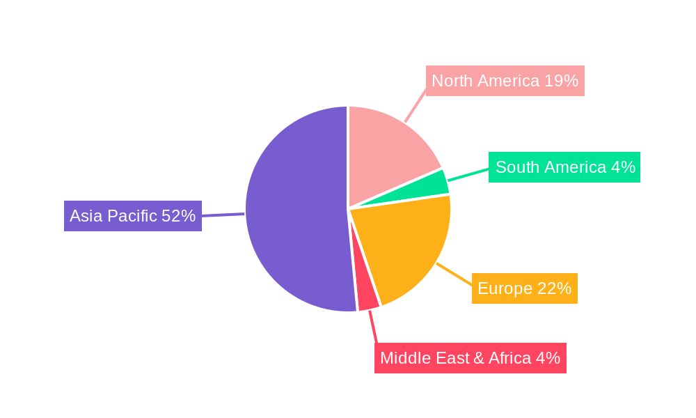
The Asia-Pacific region, particularly countries like South Korea, Taiwan, and China, stands as the dominant market for photomasks for semiconductors, accounting for an estimated 60% of the global market value. This dominance is attributed to the concentration of major semiconductor foundries and integrated device manufacturers (IDMs) in this region. Within this region, Taiwan, with its leading foundries, is a significant individual market.
Dominant Segments:
Application:
- Consumer Electronics: This segment is the largest revenue generator, driven by the massive global demand for smartphones, laptops, tablets, and gaming consoles. The continuous innovation cycle in consumer electronics necessitates frequent upgrades and the production of more powerful chips, directly boosting photomask demand. Economic policies promoting technological adoption and substantial consumer spending power contribute to its dominance.
- Telecommunication: The ongoing global rollout of 5G infrastructure and the increasing adoption of connected devices are significant growth catalysts. Advanced communication chips require intricate photomasks for their fabrication. Investments in telecommunication infrastructure and government initiatives to expand network coverage are key drivers.
Type:
- Binary Photomask: While still prevalent for less critical layers and older technology nodes, the demand for binary photomasks is gradually shifting towards more advanced types. However, their sheer volume in legacy and less advanced production lines keeps them relevant.
- Phase Shifting Mask (PSM): The increasing need for higher resolution and critical dimension (CD) control in advanced lithography has propelled the adoption of PSMs. These masks are crucial for manufacturing at sub-100nm nodes. Technological advancements in mask design and fabrication processes are critical drivers for this segment.
Photomasks For Semiconductors Product Developments
Recent product developments in photomasks for semiconductors are characterized by a relentless pursuit of higher precision and reduced defectivity. Innovations in EUV photomask blanks, advanced pellicle technologies to protect masks from particles, and novel mask inspection techniques are at the forefront. These advancements are crucial for enabling next-generation semiconductor manufacturing at nodes below 7nm, leading to smaller, faster, and more power-efficient chips. The competitive advantage lies in companies that can deliver defect-free photomasks with enhanced resolution capabilities, directly impacting chip yield and performance for applications in high-performance computing, AI, and advanced consumer electronics.
Report Scope & Segmentation Analysis
This report segment focuses on the detailed breakdown of the photomasks for semiconductors market.
- Application: The market is segmented by Consumer Electronics, Automobile, Telecommunication, Medical, IoT, and Others. Consumer Electronics and Telecommunication are projected to exhibit the highest growth rates due to their intrinsic reliance on cutting-edge semiconductor technology. The automotive sector is also a rapidly expanding segment, driven by increasing electronic content in vehicles.
- Type: The market is further categorized into Binary Photomask, Phase Shifting Mask, and Others. Phase Shifting Masks are expected to witness significant growth as semiconductor manufacturers transition to more advanced lithographic processes requiring enhanced resolution and pattern fidelity.
Key Drivers of Photomasks For Semiconductors Growth
Several key factors are propelling the growth of the photomasks for semiconductors market. The accelerating pace of technological innovation in the semiconductor industry, driven by Moore's Law and the demand for miniaturization, is a primary driver. The increasing complexity and density of integrated circuits require increasingly sophisticated photomasks. The exponential growth in demand for semiconductors across diverse sectors, including consumer electronics, automotive, telecommunications, and IoT, directly translates into a higher volume of photomask production. Government initiatives and investments in semiconductor manufacturing capabilities, particularly in emerging economies, also contribute significantly. Furthermore, the ongoing advancements in lithography techniques, such as EUV lithography, necessitate the development and use of advanced photomask technologies.
Challenges in the Photomasks For Semiconductors Sector
Despite robust growth, the photomasks for semiconductors sector faces several challenges. The extreme complexity and high cost associated with developing and manufacturing advanced photomasks, particularly EUV photomasks, present a significant barrier. Strict quality control and defectivity requirements are paramount, and any compromise can lead to substantial yield losses in chip manufacturing, estimated in the hundreds of millions of dollars per incident. Supply chain disruptions, geopolitical factors, and the limited number of qualified manufacturers can also impact availability and pricing. Intense competition and the need for continuous innovation to keep pace with shrinking semiconductor nodes require substantial capital investment. Regulatory hurdles related to intellectual property and trade compliance can also pose challenges for global market participants.
Emerging Opportunities in Photomasks For Semiconductors
The photomasks for semiconductors market is ripe with emerging opportunities. The increasing adoption of advanced packaging technologies, which often utilize specialized photomasks, presents a new avenue for growth. The burgeoning demand for semiconductors in emerging fields like artificial intelligence (AI), machine learning, and edge computing will necessitate the production of highly customized and complex chips, requiring advanced photomasks. Expansion into new geographical markets with growing semiconductor manufacturing capabilities offers significant potential. Furthermore, innovations in mask data preparation (MDP) and maskless lithography technologies could create new market segments and opportunities for service providers. The increasing focus on sustainability and energy efficiency in electronics will also drive demand for more advanced chips, indirectly boosting the photomask market.
Leading Players in the Photomasks For Semiconductors Market
- Photronics
- Toppan
- DNP
- Hoya
- SK-Electronics
- LG Innotek
- Shenzhen Qingyi Photomask Limited
- Taiwan Mask
- Nippon Filcon
- Compugraphics
- Newway Photomask
Key Developments in Photomasks For Semiconductors Industry
- 2023/09: Advancements in EUV photomask blank manufacturing by major players, improving yield and reducing defectivity.
- 2023/06: Strategic partnerships formed between photomask manufacturers and leading foundries to co-develop next-generation mask technologies.
- 2022/12: Increased investment in R&D for advanced pellicle solutions to enhance photomask protection and reduce contamination.
- 2022/08: Expansion of manufacturing capacity for advanced photomasks in Asia-Pacific to meet rising demand.
- 2021/05: Introduction of novel mask inspection and metrology tools for enhanced defect detection at sub-10nm nodes.
Strategic Outlook for Photomasks For Semiconductors Market
The strategic outlook for the photomasks for semiconductors market is exceptionally positive, driven by the foundational role these components play in the entire semiconductor ecosystem. Continued investment in R&D for cutting-edge technologies like EUV and complementary patterning techniques will be crucial for maintaining a competitive edge. Expansion of manufacturing capacity, particularly in regions with high demand, will be a key growth catalyst. Strategic collaborations and partnerships between photomask suppliers, foundries, and equipment manufacturers will foster innovation and accelerate technology adoption. The increasing importance of semiconductors in emerging applications like AI and advanced connectivity ensures sustained demand. Companies that can effectively address the challenges of cost, complexity, and defectivity while embracing new technological frontiers are poised for significant growth and market leadership in the coming years.
Photomasks For Semiconductors Segmentation
-
1. Application
- 1.1. Consumer Electronics
- 1.2. Automobile
- 1.3. Telecommunication
- 1.4. Medical
- 1.5. IoT
- 1.6. Others
-
2. Type
- 2.1. Binary Photomask
- 2.2. Phase Shifting Mask
- 2.3. Others
Photomasks For Semiconductors Segmentation By Geography
-
1. North America
- 1.1. United States
- 1.2. Canada
- 1.3. Mexico
-
2. South America
- 2.1. Brazil
- 2.2. Argentina
- 2.3. Rest of South America
-
3. Europe
- 3.1. United Kingdom
- 3.2. Germany
- 3.3. France
- 3.4. Italy
- 3.5. Spain
- 3.6. Russia
- 3.7. Benelux
- 3.8. Nordics
- 3.9. Rest of Europe
-
4. Middle East & Africa
- 4.1. Turkey
- 4.2. Israel
- 4.3. GCC
- 4.4. North Africa
- 4.5. South Africa
- 4.6. Rest of Middle East & Africa
-
5. Asia Pacific
- 5.1. China
- 5.2. India
- 5.3. Japan
- 5.4. South Korea
- 5.5. ASEAN
- 5.6. Oceania
- 5.7. Rest of Asia Pacific
Photomasks For Semiconductors REPORT HIGHLIGHTS
| Aspects | Details |
|---|---|
| Study Period | 2019-2033 |
| Base Year | 2024 |
| Estimated Year | 2025 |
| Forecast Period | 2025-2033 |
| Historical Period | 2019-2024 |
| Growth Rate | CAGR of XXX% from 2019-2033 |
| Segmentation |
|
Table of Contents
- 1. Introduction
- 1.1. Research Scope
- 1.2. Market Segmentation
- 1.3. Research Methodology
- 1.4. Definitions and Assumptions
- 2. Executive Summary
- 2.1. Introduction
- 3. Market Dynamics
- 3.1. Introduction
- 3.2. Market Drivers
- 3.3. Market Restrains
- 3.4. Market Trends
- 4. Market Factor Analysis
- 4.1. Porters Five Forces
- 4.2. Supply/Value Chain
- 4.3. PESTEL analysis
- 4.4. Market Entropy
- 4.5. Patent/Trademark Analysis
- 5. Global Photomasks For Semiconductors Analysis, Insights and Forecast, 2019-2031
- 5.1. Market Analysis, Insights and Forecast - by Application
- 5.1.1. Consumer Electronics
- 5.1.2. Automobile
- 5.1.3. Telecommunication
- 5.1.4. Medical
- 5.1.5. IoT
- 5.1.6. Others
- 5.2. Market Analysis, Insights and Forecast - by Type
- 5.2.1. Binary Photomask
- 5.2.2. Phase Shifting Mask
- 5.2.3. Others
- 5.3. Market Analysis, Insights and Forecast - by Region
- 5.3.1. North America
- 5.3.2. South America
- 5.3.3. Europe
- 5.3.4. Middle East & Africa
- 5.3.5. Asia Pacific
- 5.1. Market Analysis, Insights and Forecast - by Application
- 6. North America Photomasks For Semiconductors Analysis, Insights and Forecast, 2019-2031
- 6.1. Market Analysis, Insights and Forecast - by Application
- 6.1.1. Consumer Electronics
- 6.1.2. Automobile
- 6.1.3. Telecommunication
- 6.1.4. Medical
- 6.1.5. IoT
- 6.1.6. Others
- 6.2. Market Analysis, Insights and Forecast - by Type
- 6.2.1. Binary Photomask
- 6.2.2. Phase Shifting Mask
- 6.2.3. Others
- 6.1. Market Analysis, Insights and Forecast - by Application
- 7. South America Photomasks For Semiconductors Analysis, Insights and Forecast, 2019-2031
- 7.1. Market Analysis, Insights and Forecast - by Application
- 7.1.1. Consumer Electronics
- 7.1.2. Automobile
- 7.1.3. Telecommunication
- 7.1.4. Medical
- 7.1.5. IoT
- 7.1.6. Others
- 7.2. Market Analysis, Insights and Forecast - by Type
- 7.2.1. Binary Photomask
- 7.2.2. Phase Shifting Mask
- 7.2.3. Others
- 7.1. Market Analysis, Insights and Forecast - by Application
- 8. Europe Photomasks For Semiconductors Analysis, Insights and Forecast, 2019-2031
- 8.1. Market Analysis, Insights and Forecast - by Application
- 8.1.1. Consumer Electronics
- 8.1.2. Automobile
- 8.1.3. Telecommunication
- 8.1.4. Medical
- 8.1.5. IoT
- 8.1.6. Others
- 8.2. Market Analysis, Insights and Forecast - by Type
- 8.2.1. Binary Photomask
- 8.2.2. Phase Shifting Mask
- 8.2.3. Others
- 8.1. Market Analysis, Insights and Forecast - by Application
- 9. Middle East & Africa Photomasks For Semiconductors Analysis, Insights and Forecast, 2019-2031
- 9.1. Market Analysis, Insights and Forecast - by Application
- 9.1.1. Consumer Electronics
- 9.1.2. Automobile
- 9.1.3. Telecommunication
- 9.1.4. Medical
- 9.1.5. IoT
- 9.1.6. Others
- 9.2. Market Analysis, Insights and Forecast - by Type
- 9.2.1. Binary Photomask
- 9.2.2. Phase Shifting Mask
- 9.2.3. Others
- 9.1. Market Analysis, Insights and Forecast - by Application
- 10. Asia Pacific Photomasks For Semiconductors Analysis, Insights and Forecast, 2019-2031
- 10.1. Market Analysis, Insights and Forecast - by Application
- 10.1.1. Consumer Electronics
- 10.1.2. Automobile
- 10.1.3. Telecommunication
- 10.1.4. Medical
- 10.1.5. IoT
- 10.1.6. Others
- 10.2. Market Analysis, Insights and Forecast - by Type
- 10.2.1. Binary Photomask
- 10.2.2. Phase Shifting Mask
- 10.2.3. Others
- 10.1. Market Analysis, Insights and Forecast - by Application
- 11. Competitive Analysis
- 11.1. Global Market Share Analysis 2024
- 11.2. Company Profiles
- 11.2.1 Photronics
- 11.2.1.1. Overview
- 11.2.1.2. Products
- 11.2.1.3. SWOT Analysis
- 11.2.1.4. Recent Developments
- 11.2.1.5. Financials (Based on Availability)
- 11.2.2 Toppan
- 11.2.2.1. Overview
- 11.2.2.2. Products
- 11.2.2.3. SWOT Analysis
- 11.2.2.4. Recent Developments
- 11.2.2.5. Financials (Based on Availability)
- 11.2.3 DNP
- 11.2.3.1. Overview
- 11.2.3.2. Products
- 11.2.3.3. SWOT Analysis
- 11.2.3.4. Recent Developments
- 11.2.3.5. Financials (Based on Availability)
- 11.2.4 Hoya
- 11.2.4.1. Overview
- 11.2.4.2. Products
- 11.2.4.3. SWOT Analysis
- 11.2.4.4. Recent Developments
- 11.2.4.5. Financials (Based on Availability)
- 11.2.5 SK-Electronics
- 11.2.5.1. Overview
- 11.2.5.2. Products
- 11.2.5.3. SWOT Analysis
- 11.2.5.4. Recent Developments
- 11.2.5.5. Financials (Based on Availability)
- 11.2.6 LG Innotek
- 11.2.6.1. Overview
- 11.2.6.2. Products
- 11.2.6.3. SWOT Analysis
- 11.2.6.4. Recent Developments
- 11.2.6.5. Financials (Based on Availability)
- 11.2.7 Shenzhen Qingyi Photomask Limited
- 11.2.7.1. Overview
- 11.2.7.2. Products
- 11.2.7.3. SWOT Analysis
- 11.2.7.4. Recent Developments
- 11.2.7.5. Financials (Based on Availability)
- 11.2.8 Taiwan Mask
- 11.2.8.1. Overview
- 11.2.8.2. Products
- 11.2.8.3. SWOT Analysis
- 11.2.8.4. Recent Developments
- 11.2.8.5. Financials (Based on Availability)
- 11.2.9 Nippon Filcon
- 11.2.9.1. Overview
- 11.2.9.2. Products
- 11.2.9.3. SWOT Analysis
- 11.2.9.4. Recent Developments
- 11.2.9.5. Financials (Based on Availability)
- 11.2.10 Compugraphics
- 11.2.10.1. Overview
- 11.2.10.2. Products
- 11.2.10.3. SWOT Analysis
- 11.2.10.4. Recent Developments
- 11.2.10.5. Financials (Based on Availability)
- 11.2.11 Newway Photomask
- 11.2.11.1. Overview
- 11.2.11.2. Products
- 11.2.11.3. SWOT Analysis
- 11.2.11.4. Recent Developments
- 11.2.11.5. Financials (Based on Availability)
- 11.2.1 Photronics
List of Figures
- Figure 1: Global Photomasks For Semiconductors Revenue Breakdown (million, %) by Region 2024 & 2032
- Figure 2: North America Photomasks For Semiconductors Revenue (million), by Application 2024 & 2032
- Figure 3: North America Photomasks For Semiconductors Revenue Share (%), by Application 2024 & 2032
- Figure 4: North America Photomasks For Semiconductors Revenue (million), by Type 2024 & 2032
- Figure 5: North America Photomasks For Semiconductors Revenue Share (%), by Type 2024 & 2032
- Figure 6: North America Photomasks For Semiconductors Revenue (million), by Country 2024 & 2032
- Figure 7: North America Photomasks For Semiconductors Revenue Share (%), by Country 2024 & 2032
- Figure 8: South America Photomasks For Semiconductors Revenue (million), by Application 2024 & 2032
- Figure 9: South America Photomasks For Semiconductors Revenue Share (%), by Application 2024 & 2032
- Figure 10: South America Photomasks For Semiconductors Revenue (million), by Type 2024 & 2032
- Figure 11: South America Photomasks For Semiconductors Revenue Share (%), by Type 2024 & 2032
- Figure 12: South America Photomasks For Semiconductors Revenue (million), by Country 2024 & 2032
- Figure 13: South America Photomasks For Semiconductors Revenue Share (%), by Country 2024 & 2032
- Figure 14: Europe Photomasks For Semiconductors Revenue (million), by Application 2024 & 2032
- Figure 15: Europe Photomasks For Semiconductors Revenue Share (%), by Application 2024 & 2032
- Figure 16: Europe Photomasks For Semiconductors Revenue (million), by Type 2024 & 2032
- Figure 17: Europe Photomasks For Semiconductors Revenue Share (%), by Type 2024 & 2032
- Figure 18: Europe Photomasks For Semiconductors Revenue (million), by Country 2024 & 2032
- Figure 19: Europe Photomasks For Semiconductors Revenue Share (%), by Country 2024 & 2032
- Figure 20: Middle East & Africa Photomasks For Semiconductors Revenue (million), by Application 2024 & 2032
- Figure 21: Middle East & Africa Photomasks For Semiconductors Revenue Share (%), by Application 2024 & 2032
- Figure 22: Middle East & Africa Photomasks For Semiconductors Revenue (million), by Type 2024 & 2032
- Figure 23: Middle East & Africa Photomasks For Semiconductors Revenue Share (%), by Type 2024 & 2032
- Figure 24: Middle East & Africa Photomasks For Semiconductors Revenue (million), by Country 2024 & 2032
- Figure 25: Middle East & Africa Photomasks For Semiconductors Revenue Share (%), by Country 2024 & 2032
- Figure 26: Asia Pacific Photomasks For Semiconductors Revenue (million), by Application 2024 & 2032
- Figure 27: Asia Pacific Photomasks For Semiconductors Revenue Share (%), by Application 2024 & 2032
- Figure 28: Asia Pacific Photomasks For Semiconductors Revenue (million), by Type 2024 & 2032
- Figure 29: Asia Pacific Photomasks For Semiconductors Revenue Share (%), by Type 2024 & 2032
- Figure 30: Asia Pacific Photomasks For Semiconductors Revenue (million), by Country 2024 & 2032
- Figure 31: Asia Pacific Photomasks For Semiconductors Revenue Share (%), by Country 2024 & 2032
List of Tables
- Table 1: Global Photomasks For Semiconductors Revenue million Forecast, by Region 2019 & 2032
- Table 2: Global Photomasks For Semiconductors Revenue million Forecast, by Application 2019 & 2032
- Table 3: Global Photomasks For Semiconductors Revenue million Forecast, by Type 2019 & 2032
- Table 4: Global Photomasks For Semiconductors Revenue million Forecast, by Region 2019 & 2032
- Table 5: Global Photomasks For Semiconductors Revenue million Forecast, by Application 2019 & 2032
- Table 6: Global Photomasks For Semiconductors Revenue million Forecast, by Type 2019 & 2032
- Table 7: Global Photomasks For Semiconductors Revenue million Forecast, by Country 2019 & 2032
- Table 8: United States Photomasks For Semiconductors Revenue (million) Forecast, by Application 2019 & 2032
- Table 9: Canada Photomasks For Semiconductors Revenue (million) Forecast, by Application 2019 & 2032
- Table 10: Mexico Photomasks For Semiconductors Revenue (million) Forecast, by Application 2019 & 2032
- Table 11: Global Photomasks For Semiconductors Revenue million Forecast, by Application 2019 & 2032
- Table 12: Global Photomasks For Semiconductors Revenue million Forecast, by Type 2019 & 2032
- Table 13: Global Photomasks For Semiconductors Revenue million Forecast, by Country 2019 & 2032
- Table 14: Brazil Photomasks For Semiconductors Revenue (million) Forecast, by Application 2019 & 2032
- Table 15: Argentina Photomasks For Semiconductors Revenue (million) Forecast, by Application 2019 & 2032
- Table 16: Rest of South America Photomasks For Semiconductors Revenue (million) Forecast, by Application 2019 & 2032
- Table 17: Global Photomasks For Semiconductors Revenue million Forecast, by Application 2019 & 2032
- Table 18: Global Photomasks For Semiconductors Revenue million Forecast, by Type 2019 & 2032
- Table 19: Global Photomasks For Semiconductors Revenue million Forecast, by Country 2019 & 2032
- Table 20: United Kingdom Photomasks For Semiconductors Revenue (million) Forecast, by Application 2019 & 2032
- Table 21: Germany Photomasks For Semiconductors Revenue (million) Forecast, by Application 2019 & 2032
- Table 22: France Photomasks For Semiconductors Revenue (million) Forecast, by Application 2019 & 2032
- Table 23: Italy Photomasks For Semiconductors Revenue (million) Forecast, by Application 2019 & 2032
- Table 24: Spain Photomasks For Semiconductors Revenue (million) Forecast, by Application 2019 & 2032
- Table 25: Russia Photomasks For Semiconductors Revenue (million) Forecast, by Application 2019 & 2032
- Table 26: Benelux Photomasks For Semiconductors Revenue (million) Forecast, by Application 2019 & 2032
- Table 27: Nordics Photomasks For Semiconductors Revenue (million) Forecast, by Application 2019 & 2032
- Table 28: Rest of Europe Photomasks For Semiconductors Revenue (million) Forecast, by Application 2019 & 2032
- Table 29: Global Photomasks For Semiconductors Revenue million Forecast, by Application 2019 & 2032
- Table 30: Global Photomasks For Semiconductors Revenue million Forecast, by Type 2019 & 2032
- Table 31: Global Photomasks For Semiconductors Revenue million Forecast, by Country 2019 & 2032
- Table 32: Turkey Photomasks For Semiconductors Revenue (million) Forecast, by Application 2019 & 2032
- Table 33: Israel Photomasks For Semiconductors Revenue (million) Forecast, by Application 2019 & 2032
- Table 34: GCC Photomasks For Semiconductors Revenue (million) Forecast, by Application 2019 & 2032
- Table 35: North Africa Photomasks For Semiconductors Revenue (million) Forecast, by Application 2019 & 2032
- Table 36: South Africa Photomasks For Semiconductors Revenue (million) Forecast, by Application 2019 & 2032
- Table 37: Rest of Middle East & Africa Photomasks For Semiconductors Revenue (million) Forecast, by Application 2019 & 2032
- Table 38: Global Photomasks For Semiconductors Revenue million Forecast, by Application 2019 & 2032
- Table 39: Global Photomasks For Semiconductors Revenue million Forecast, by Type 2019 & 2032
- Table 40: Global Photomasks For Semiconductors Revenue million Forecast, by Country 2019 & 2032
- Table 41: China Photomasks For Semiconductors Revenue (million) Forecast, by Application 2019 & 2032
- Table 42: India Photomasks For Semiconductors Revenue (million) Forecast, by Application 2019 & 2032
- Table 43: Japan Photomasks For Semiconductors Revenue (million) Forecast, by Application 2019 & 2032
- Table 44: South Korea Photomasks For Semiconductors Revenue (million) Forecast, by Application 2019 & 2032
- Table 45: ASEAN Photomasks For Semiconductors Revenue (million) Forecast, by Application 2019 & 2032
- Table 46: Oceania Photomasks For Semiconductors Revenue (million) Forecast, by Application 2019 & 2032
- Table 47: Rest of Asia Pacific Photomasks For Semiconductors Revenue (million) Forecast, by Application 2019 & 2032
Frequently Asked Questions
1. What is the projected Compound Annual Growth Rate (CAGR) of the Photomasks For Semiconductors?
The projected CAGR is approximately XXX%.
2. Which companies are prominent players in the Photomasks For Semiconductors?
Key companies in the market include Photronics, Toppan, DNP, Hoya, SK-Electronics, LG Innotek, Shenzhen Qingyi Photomask Limited, Taiwan Mask, Nippon Filcon, Compugraphics, Newway Photomask.
3. What are the main segments of the Photomasks For Semiconductors?
The market segments include Application, Type.
4. Can you provide details about the market size?
The market size is estimated to be USD XXX million as of 2022.
5. What are some drivers contributing to market growth?
N/A
6. What are the notable trends driving market growth?
N/A
7. Are there any restraints impacting market growth?
N/A
8. Can you provide examples of recent developments in the market?
N/A
9. What pricing options are available for accessing the report?
Pricing options include single-user, multi-user, and enterprise licenses priced at USD 4250.00, USD 6375.00, and USD 8500.00 respectively.
10. Is the market size provided in terms of value or volume?
The market size is provided in terms of value, measured in million.
11. Are there any specific market keywords associated with the report?
Yes, the market keyword associated with the report is "Photomasks For Semiconductors," which aids in identifying and referencing the specific market segment covered.
12. How do I determine which pricing option suits my needs best?
The pricing options vary based on user requirements and access needs. Individual users may opt for single-user licenses, while businesses requiring broader access may choose multi-user or enterprise licenses for cost-effective access to the report.
13. Are there any additional resources or data provided in the Photomasks For Semiconductors report?
While the report offers comprehensive insights, it's advisable to review the specific contents or supplementary materials provided to ascertain if additional resources or data are available.
14. How can I stay updated on further developments or reports in the Photomasks For Semiconductors?
To stay informed about further developments, trends, and reports in the Photomasks For Semiconductors, consider subscribing to industry newsletters, following relevant companies and organizations, or regularly checking reputable industry news sources and publications.
Methodology
Step 1 - Identification of Relevant Samples Size from Population Database


Step 2 - Approaches for Defining Global Market Size (Value, Volume* & Price*)

Note*: In applicable scenarios
Step 3 - Data Sources
Primary Research
- Web Analytics
- Survey Reports
- Research Institute
- Latest Research Reports
- Opinion Leaders
Secondary Research
- Annual Reports
- White Paper
- Latest Press Release
- Industry Association
- Paid Database
- Investor Presentations

Step 4 - Data Triangulation
Involves using different sources of information in order to increase the validity of a study
These sources are likely to be stakeholders in a program - participants, other researchers, program staff, other community members, and so on.
Then we put all data in single framework & apply various statistical tools to find out the dynamic on the market.
During the analysis stage, feedback from the stakeholder groups would be compared to determine areas of agreement as well as areas of divergence


